

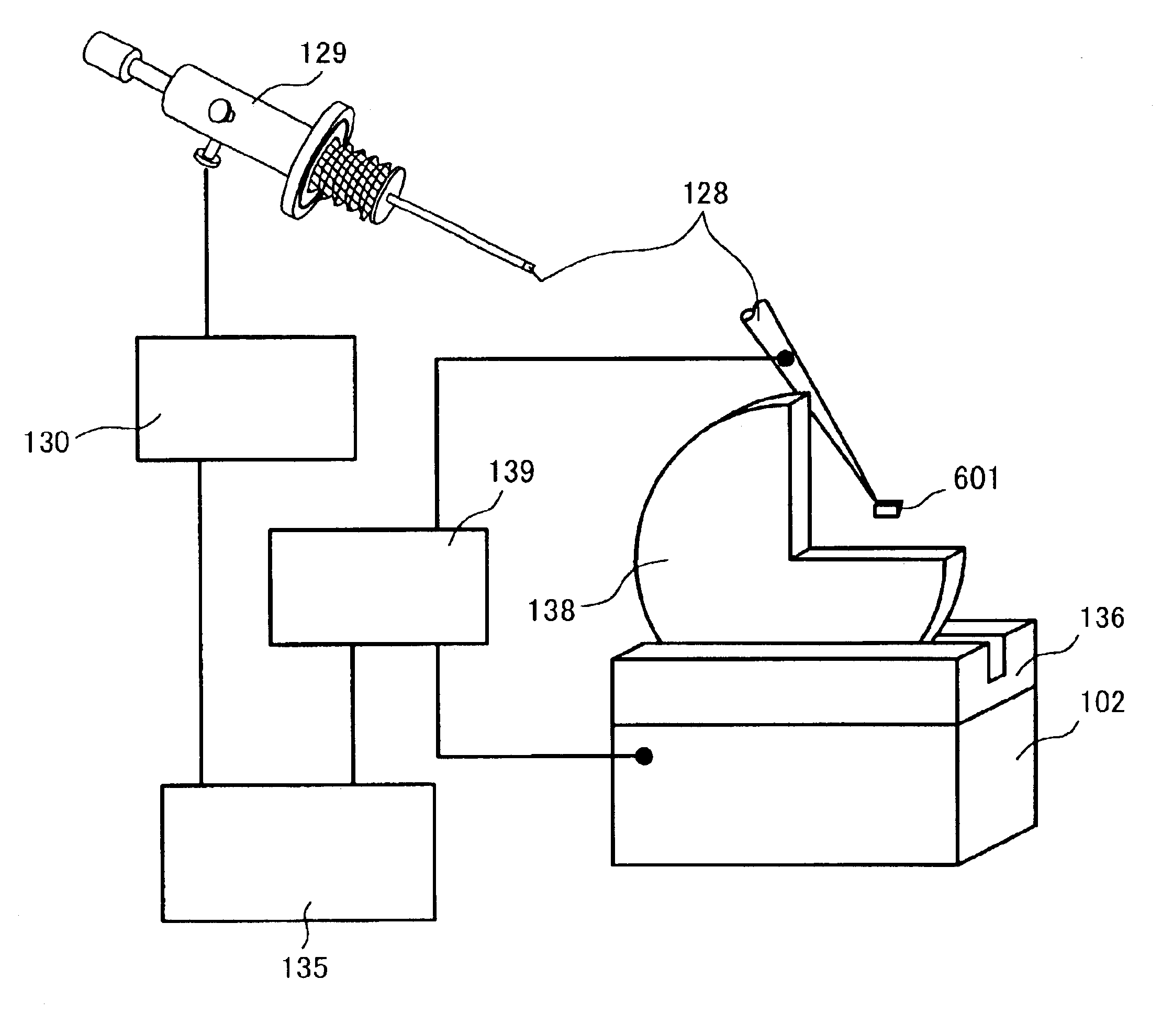
Apparatus for specimen fabrication and method for specimen fabrication
a technology of apparatus and specimen, applied in the direction of material analysis using wave/particle radiation, instruments, nuclear engineering, etc., can solve the problem that it is difficult to shorten the sample preparation time, and the quality of the observation object to be subjected to a failure analysis cannot be denied
- Summary
- Abstract
- Description
- Claims
- Application Information
AI Technical Summary
Benefits of technology
Problems solved by technology
Method used
Image

Examples
Embodiment Construction
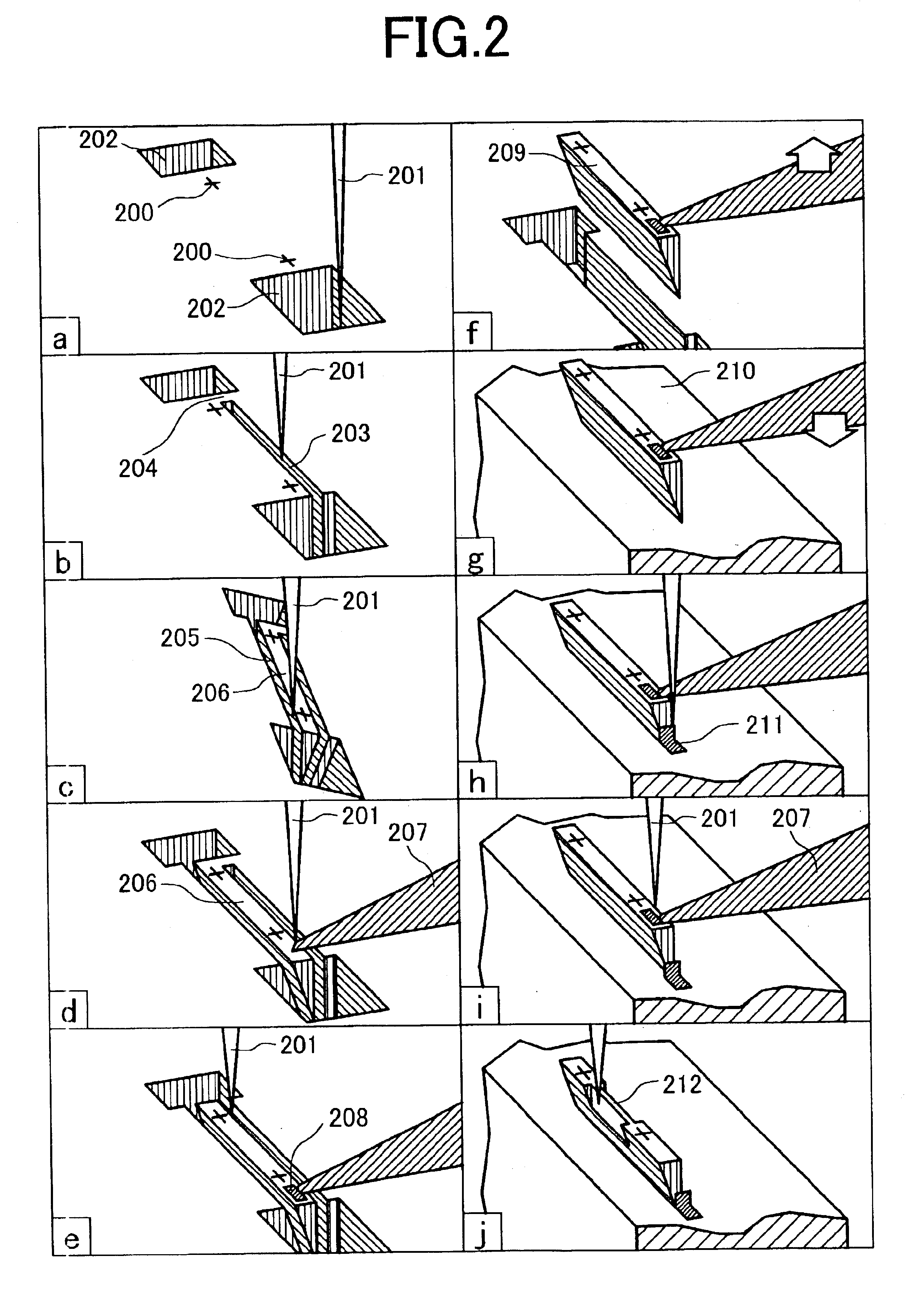
9(a) to 9(j) are flow diagrams showing one preferred embodiment of a microfabrication method according to the present invention;
[0040]FIGS. 10A and 10B are diagrams showing observation states of a micro-sample according to the preferred embodiment of the present invention;
[0041]FIGS. 11A and 11B are diagrams showing a processing method for a shallow micro-sample (forming only membrane);
[0042]FIGS. 12A to 12D are diagrams showing a processing method for a shallow micro-sample (processing membrane later);
[0043]FIGS. 13A and 13B are diagrams respectively showing methods of fixing a plurality of micro-samples to one micro-sample holder;
[0044]FIG. 14 is a diagram showing a method of fixing a plurality of micro-samples to one micro-sample holder according to one preferred embodiment of the present invention;
[0045]FIGS. 15A to 15D are diagrams showing the flow of welding a micro-sample to a micro-sample holder;
[0046]FIGS. 16A and 16B are diagrams showing a technique of welding a probe and ...
PUM
| Property | Measurement | Unit |
|---|---|---|
| voltage | aaaaa | aaaaa |
| height | aaaaa | aaaaa |
| thickness | aaaaa | aaaaa |
Abstract
Description
Claims
Application Information