Method of fabricating a molded package for micromechanical devices

a micromechanical device and packaging technology, applied in the direction of micromechanical device details, instruments, acceleration measurement using interia forces, etc., can solve the problems of low package cost, high cost of overall package structure, application and removal of micromechanical devices, etc., to avoid downtime and cost, avoid the effect of high cost and unusual flat surfa

Inactive Publication Date: 2005-02-22
TEXAS INSTR INC
View PDF13 Cites 59 Cited by
  • Summary
  • Abstract
  • Description
  • Claims
  • Application Information

AI Technical Summary

Benefits of technology

Another aspect of the invention is to provide ultra-thin devices free of any voids in the molded portions, and having unusually flat surfaces and high luster. The invention solves these needs by modifying the “3-P” molding technique with its film

Problems solved by technology

Today's overall package structure for micromechanical devices and method of fabrication is expensive.
This fact is in conflict with the market requirements for many applications of micromechanical devices, which put a premium at low device cost and, therefore, low package cost.
Its application and removal exhibit manufa

Method used


Image

  • Method of fabricating a molded package for micromechanical devices
  • Method of fabricating a molded package for micromechanical devices
  • Method of fabricating a molded package for micromechanical devices

Examples


Embodiment Construction

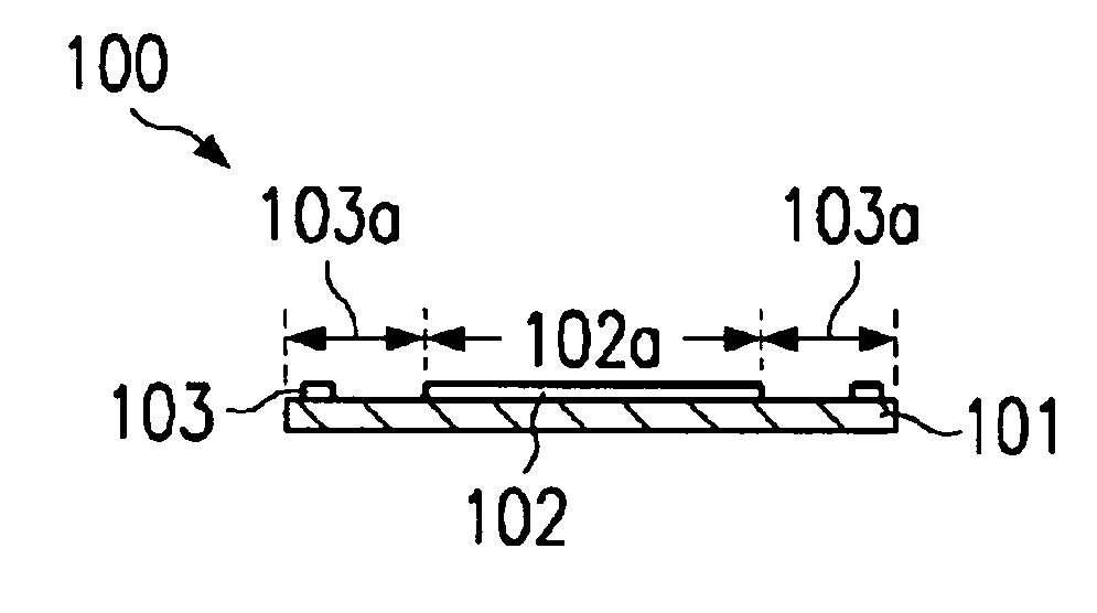
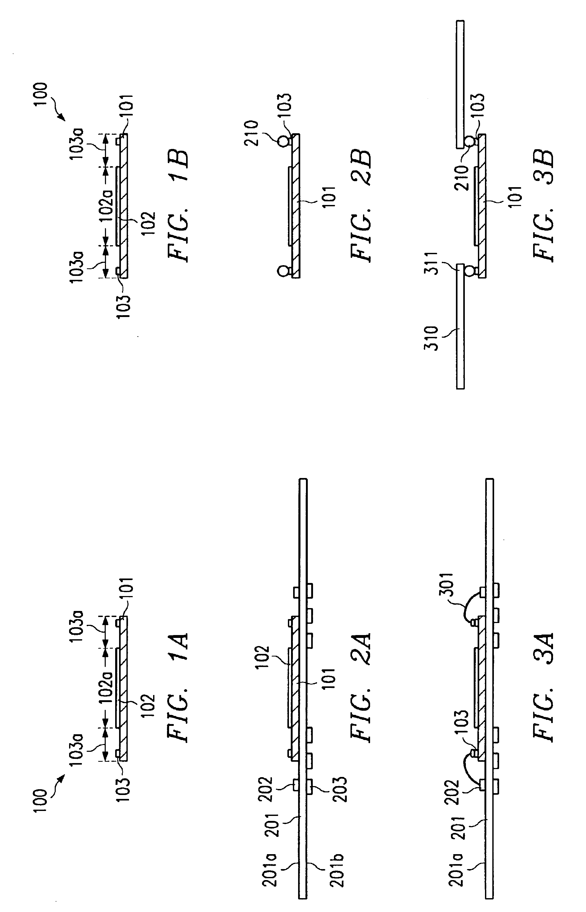
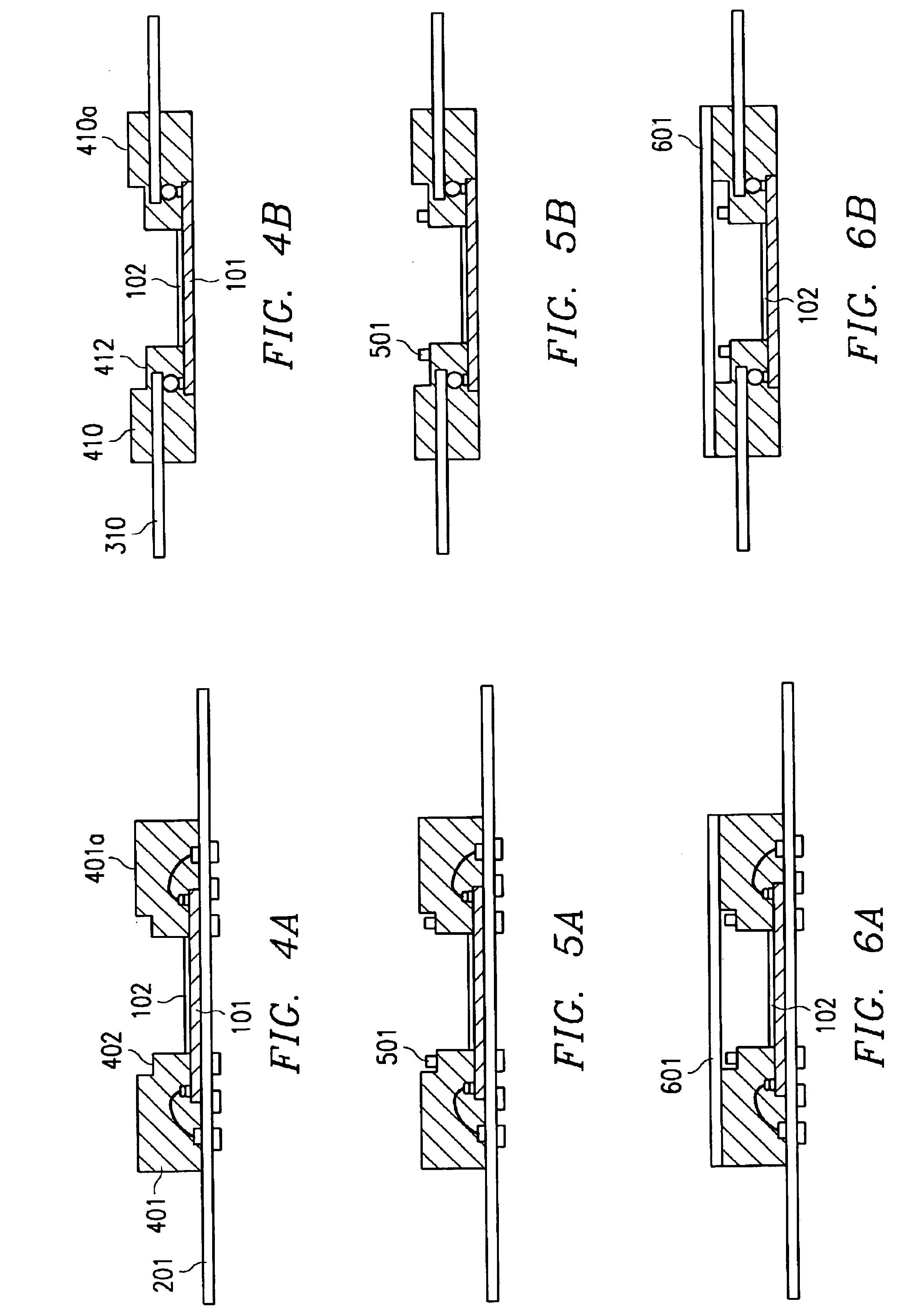
The present invention adopts essential features of the so-called “3-P” molding technology and modifies them for preferred embodiments as illustrated in FIGS. 1A to 7A and 1B to 7B.

The term “3-P” refers to the concept of using material as “pre-packaged product”. The encapsulation material is carefully cleaned from impurities and gaseous contents, and thereafter wrapped in thin plastic films. With this protection from the environment, the material is shipped to the customer, who can use it in clean condition. The wrapped product may be fabricated in various geometrical forms, for instance in elongated, narrow shapes reminiscent of pencils. Such “pencils” are preferred shapes of encapsulation due to their ease of operation in transfer molding.

The transfer molding technology was introduced to semiconductor devices (U.S. Pat. Nos. 3,716,764 and 4,043,027) as an encapsulation process, which is both gentle and reliable, and exceedingly well applicable to mass production. Over the years, tr...


PUM

PropertyMeasurementUnit
Flexibilityaaaaaaaaaa
Sensitivityaaaaaaaaaa

Abstract

A plastic land-grid array package, a ball-grid array package, and a plastic leaded package for micromechanical components are fabricated by a molding process characterized by lining the cavity surfaces of the top and bottom mold halves with a protective plastic film, which also protects the surfaces of the components during the molding phase, selectively encapsulating the bonding pads and coupling members of the chip while leaving empty space above the components, and attaching a lid over the components. A molding method as well as a molding apparatus are provided compatible with the sensitivity of the micromechanical devices, yet flexible with regard to the technique used to assemble the chip and the substrate. Furthermore, the method disclosed is flexible with regard to the material and the properties of the substrate.
It is an aspect of the present invention to be applicable to a variety of different semiconductor micromechanical devices, for instance actuators, motors, sensors, spatial light modulators, and deformable mirror devices. In all applications, the invention achieves technical advantages as well as significant cost reduction and yield increase.

Description

FIELD OF THE INVENTIONThe present invention is related in general to the field of semiconductor devices and processes and more specifically to the fabrication of a molded package suitable generally for micromechanical devices and specifically for digital mirror devices.DESCRIPTION OF THE RELATED ARTMicromechanical devices include actuators, motors, sensors, spatial light modulators (SLM), digital micromirror devices or deformable mirror devices (DMD), and others. The technical potential of these devices is especially evident when the devices are integrated with semiconductor circuitry using the miniaturization capability of semiconductor technology.SLMs are transducers that modulate incident light in a special pattern pursuant to an electrical or other input. The incident light may be modulated in phase, intensity, polarization or direction. SLMs of the deformable mirror class include micromechanical arrays of electronically addressable mirror elements or pixels, which are selective...

Claims


Application Information

Patent Timeline
IPC IPC(8): B29C45/14B81B7/00H01L21/56H01L23/31H01L21/02H01L23/28
CPCB29C45/14655B81C1/00333H01L21/565H01L23/3107H01L2924/10253B81C2203/0154H01L2224/48091H01L2224/48227H01L2924/01004H01L2924/01046H01L2924/01078H01L2924/01079H01L2924/15311H01L2924/1815B29C2045/14663H01L2924/01047H01L24/48H01L2924/01087H01L2224/16245H01L2924/01327H01L2224/45147H01L2924/01015H01L2924/00014H01L2924/00H01L2224/45015H01L2924/15747H01L2224/45124H01L2224/45144H01L2924/12042H01L2924/14H01L2224/05573H01L2224/05568H01L2224/05624H01L2224/05647H01L2924/181H01L24/45H01L2224/45014H01L2924/20751H01L2924/20752H01L2924/20753H01L2924/013H01L2924/00013H01L2224/05599H01L2924/00012H01L2924/206
Inventor COYLE, ANTHONY L.BEDNARZ, GEORGE A.
Owner TEXAS INSTR INC
Why Eureka
Try Eureka