Multi-chip stack and method of fabrication utilizing self-aligning electrical contact array

a technology of electrical contact array and multi-chip stack, which is applied in the direction of electrical apparatus, semiconductor devices, semiconductor/solid-state device details, etc., can solve the problems of wrong electrical connection misinterconnection between the two chips, and non-functional multi-chip stack

Inactive Publication Date: 2005-02-22
IBM CORP
View PDF27 Cites 25 Cited by
  • Summary
  • Abstract
  • Description
  • Claims
  • Application Information

AI Technical Summary

Benefits of technology

Although principally described hereinbelow with reference to a dual-chip stack structure, the electrical interconnection concepts of the present invention ca...

Problems solved by technology

A reduced size/pitch solder bump array does present a substantial challenge for a dual-chip stack assembly in that slight misalignment of the two chips could result in a mis-interconnection between the two chips, i.e. one chip could be shifted relative to the other chip resulting in having the wrong electrical connections between the two chips.
This would probably result in a non-functional mu...

Method used


Image

  • Multi-chip stack and method of fabrication utilizing self-aligning electrical contact array
  • Multi-chip stack and method of fabrication utilizing self-aligning electrical contact array
  • Multi-chip stack and method of fabrication utilizing self-aligning electrical contact array

Examples


Embodiment Construction

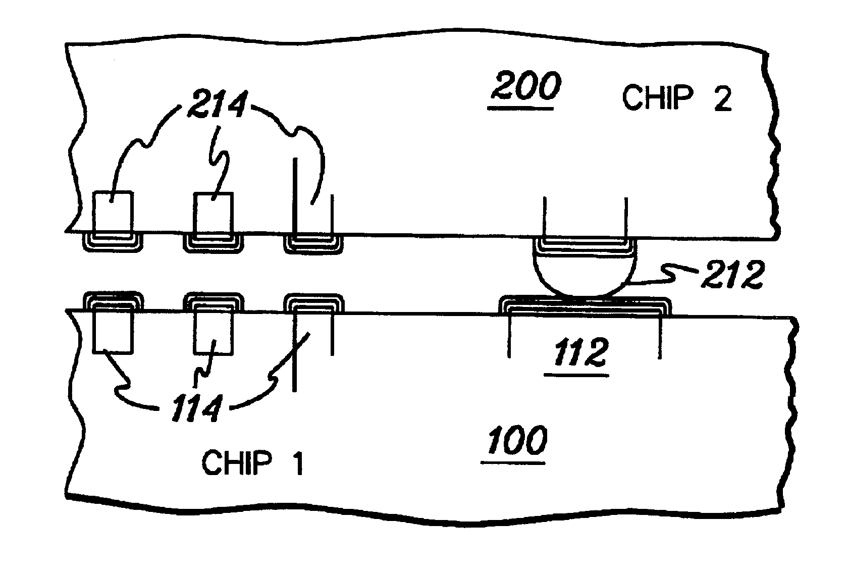
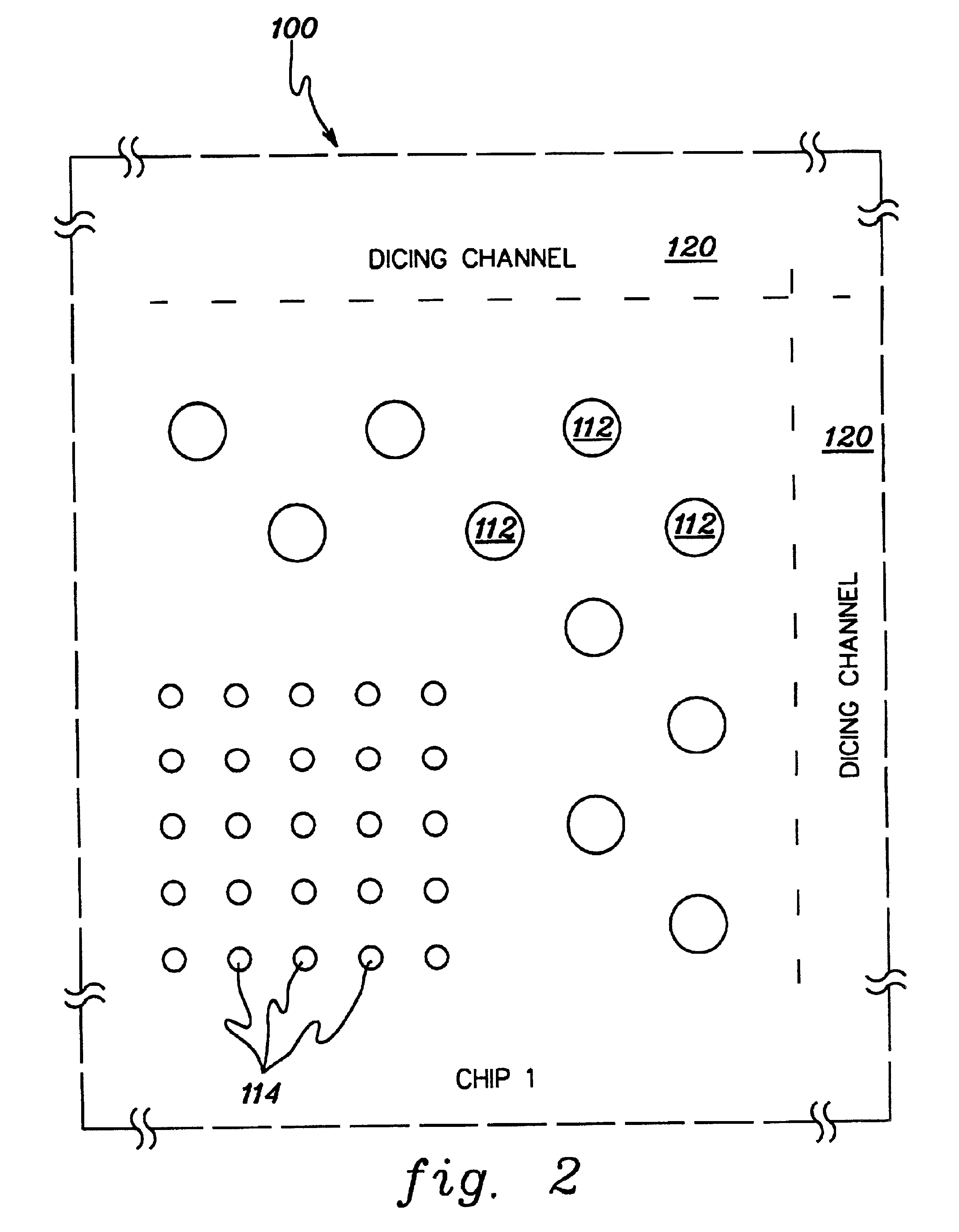
Generally stated, the present invention comprises a self-aligning electrical interconnection approach for connecting, for example, a first integrated circuit chip and a second integrated circuit chip in a dual-chip stack configuration. This self-aligning interconnection approach employs two or more interconnection arrays, with one array comprising a rough aligned contact array, and a second array comprising a high bandwidth contact array, wherein the rough aligned contact array comprises larger contacts than the contacts of the high bandwidth contact array. As described further below, the rough aligned contact array is fabricated so that the contacts have a lower melting point than the contacts of the high bandwidth contact array. Therefore, by mounting, for example, a first integrated circuit chip on top of a second integrated circuit chip and heating to melt the contacts of the rough aligned contact array, the two chips will rotate to align their respective contacts of the high ba...


PUM


Abstract

A multi-chip stack structure and method of fabrication are provided utilizing self-aligning electrical contact arrays. Two or more arrays of interconnection contacts are provided, with one array being a rough aligned contact array, and a second array being a high bandwidth contact array. The rough aligned contact array has larger contacts and at least a portion thereof which melts at a substantially lower temperature than the melting temperature of the contacts of the high bandwidth contact array. By positioning two integrated circuit chips in opposing relation with the arrays mechanically aligned therebetween, and applying heat to melt the contacts of the rough aligned array, the two chips will rotate to align the respective contacts of the high bandwidth contact arrays, thereby achieving improved connection reliability between the structures.

Description

TECHNICAL FIELDThe present invention relates in general to high density electronic packaging, and more particularly, to a multi-chip stack structure and fabrication approach employing multiple arrays of electrical contacts that are self-aligning to improve reliability and manufacturability of the structure.BACKGROUND OF THE INVENTIONSince the development of integrated circuit technology, computers and computer storage devices have been made from integrated circuit chips formed from wafers of semiconductor material. After a wafer is made, the chips are typically separated from each other by dicing the wafer. Thereafter, the individual chips are bonded to carriers of various types, interconnected by wires and packaged. As technology enhancements increase, more circuits are required per chip. This is typically accomplished by (a) making the circuits smaller and (b) making the chips larger. However, there is a practical limit to both. Making chips larger requires larger field size optic...

Claims


Application Information

Patent Timeline
IPC IPC(8): H01L25/065H01L21/02H01L21/60H01L23/485H01L23/48
CPCH01L24/11H01L24/81H01L25/0657H01L24/13H01L24/14H01L2224/14051H01L2224/13099H01L2224/13111H01L2224/81801H01L2225/06513H01L2225/06527H01L2924/01029H01L2924/01078H01L2924/01079H01L2924/01082H01L2924/01322H01L2924/14H01L2924/01005H01L2924/01006H01L2924/01033H01L2924/0105H01L2924/014H01L2224/1403H01L2224/05024H01L2224/05008H01L2224/05022H01L2224/0508H01L2224/05568H01L2224/05023H01L2224/05001H01L2224/14177H01L2224/14505H01L2224/14132H01L2224/14133H01L2224/14136H01L2224/17515H01L2224/17051H01L24/17H01L2224/14135H01L24/05H01L24/06H01L2224/0615H01L2224/0603H01L2224/05644H01L2924/00014H01L2224/05147H01L2224/05155
Inventor FERENCE, THOMAS GEORGEHOWELL, WAYNE JOHN
Owner IBM CORP
Why Eureka
Try Eureka