Method of forming silicidation blocking layer

a technology of silicidation and blocking layer, which is applied in the field of method, can solve the problems of increasing rc time delay and ir voltage drop, and achieve the effect of preventing diffusion and redistribution of impurities

Inactive Publication Date: 2005-03-01
SAMSUNG ELECTRONICS CO LTD
View PDF4 Cites 36 Cited by
  • Summary
  • Abstract
  • Description
  • Claims
  • Application Information

AI Technical Summary

Benefits of technology

The present invention has been made to solve the afore-mentioned problem, and accordingly it is an object of the present invention to provide a method of manufacturing a semiconductor device in which a silicidation blocking layer is deposited at a low temperature to prevent the diffusion of impurities in gate and source / drain regions.
According to the present invention, silicon oxynitride (SiON) is deposited at the temperature of less than 400 Celsius Degrees by the PE-CVD process to form the silicidation blocking layer. Accordingly, it is possible to prevent the diffusion and redistribution of impurities in gate and source / drain regions of the transistor during the deposition of the silicidation blocking layer.

Problems solved by technology

However, as patterns are gradually smaller, the resistivity of the polysilicon becomes higher, resulting in increasing RC time delays and IR voltage drops.

Method used


Image

  • Method of forming silicidation blocking layer
  • Method of forming silicidation blocking layer
  • Method of forming silicidation blocking layer

Examples


Embodiment Construction

Hereinafter, the preferred embodiments of the present invention will be described in detail with reference to the accompanying drawings.

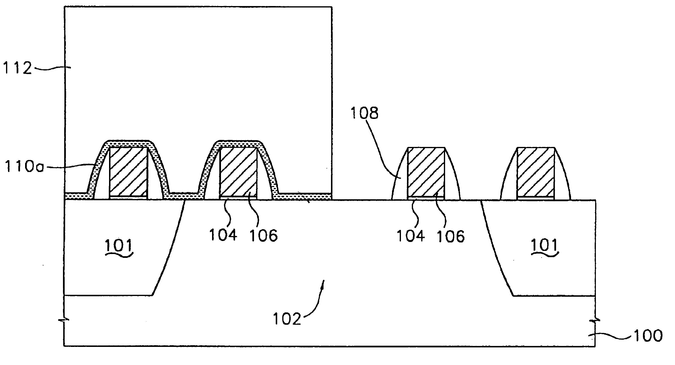
FIGS. 2A to 2E are sectional views of illustrating a method of manufacturing a logic device having a silicidation blocking layer according to one embodiment of the present invention.

FIG. 2A shows a step of forming MOS transistors. First, a semiconductor substrate 100 such as a silicon substrate is prepared. Next, a field oxide layer 101 is formed on the substrate 100 by a conventional shallow trench isolation process to thereby define an active region 102 on the substrate 100.

Next, a gate oxide layer 104 comprising silicon oxide (SiO2) or silicon oxynitride (SiON) is formed to a thickness of about 60˜80 Å on the surface of the substrate 100 in the active region 102 enclosed by the field oxide layer 101. A polysilicon layer is deposited to a thickness of about 2000˜2500 Å on the gate oxide layer 104 by a low-pressure chemical vapor deposition (LPCVD)...


PUM

PropertyMeasurementUnit
temperatureaaaaaaaaaa
temperaturesaaaaaaaaaa
temperatureaaaaaaaaaa

Abstract

Disclosed is a method of manufacturing a semiconductor device. First, a silicidation blocking layer is formed on a semiconductor substrate by a plasma enhanced chemical vapor deposition process. Next, the silicidation blocking layer in a region in which a metal silicide contact is to be formed is removed by a wet etching process. Next, after a metal layer is formed on the resultant, the silicon in the region and the metal of the metal layer are reacted to form the metal silicide. Since the silicidation blocking layer consisting of PE-SiON is formed at a low temperature of less than 400 Celsius Degrees, it is possible to prevent diffusion and redistribution of impurities in gate and source / drain regions of a transistor during the deposition of the silicidation blocking layer.

Description

BACKGROUND OF THE INVENTION1. Field of the InventionThe present invention relates to a method of manufacturing a semiconductor device, and more particularly, to a method of manufacturing a semiconductor device, which can accomplish the selective silicidation of a desired region on a semiconductor substrate.2. Description of the Related ArtAs a semiconductor device has been developed to have a high degree of integration, patterns formed on a chip become smaller in size and the gap between the patterns becomes narrower. In the past, polysilicon has been a very useful material as a wiring material such as a gate electrode or a bit line. However, as patterns are gradually smaller, the resistivity of the polysilicon becomes higher, resulting in increasing RC time delays and IR voltage drops. In order to improve short channel and punchthrough effects caused by a decrease of a gate length of the transistor, the junction depths of source / drain regions should be thinner while parasitic resis...

Claims


Application Information

Patent Timeline
Patent Type & Authority Patents(United States)
IPC IPC(8): H01L21/285H01L21/70H01L21/02H01L21/336H01L29/40H01L29/49H01L21/8234H01L21/205H01L21/311
CPCH01L21/28518H01L21/31111H01L29/665H01L29/4933H01L21/823418
Inventor PARK, JUNG-HOON
Owner SAMSUNG ELECTRONICS CO LTD
Why Eureka
Try Eureka