Silicon-on-insulator diodes and ESD protection circuits

a technology of silicon-on-insulator diodes and protection circuits, applied in the direction of electric/magnetic computing, pulse techniques, instruments, etc., can solve the problems of increasing device heating, accelerating thermal runaway, and accelerating thermal runaway, so as to improve the protection level of electrical overstress/electrostatic discharge, the effect of reducing power density and heating

Inactive Publication Date: 2005-03-01
UNITED MICROELECTRONICS CORP
View PDF5 Cites 45 Cited by
  • Summary
  • Abstract
  • Description
  • Claims
  • Application Information

AI Technical Summary

Benefits of technology

It is one object of the present invention to provide a silicon-on-insulator diode with more junction area than a normal one, thereby a lower power density and heating are obtained, and the protection level offered for electrical overstress (EOS) / electrostatic discharge (ESD) is improved.

Problems solved by technology

The device failure is initiated by thermal runaway and is followed by catastrophic damage during an ESD pulse.
In SOI devices, the presence of the buried oxide layer having a thermal conductivity {fraction (1 / 100)}th of Si causes increased device heating, which in turn accelerates thermal runaway.

Method used


Image

  • Silicon-on-insulator diodes and ESD protection circuits
  • Silicon-on-insulator diodes and ESD protection circuits
  • Silicon-on-insulator diodes and ESD protection circuits

Examples


Embodiment Construction

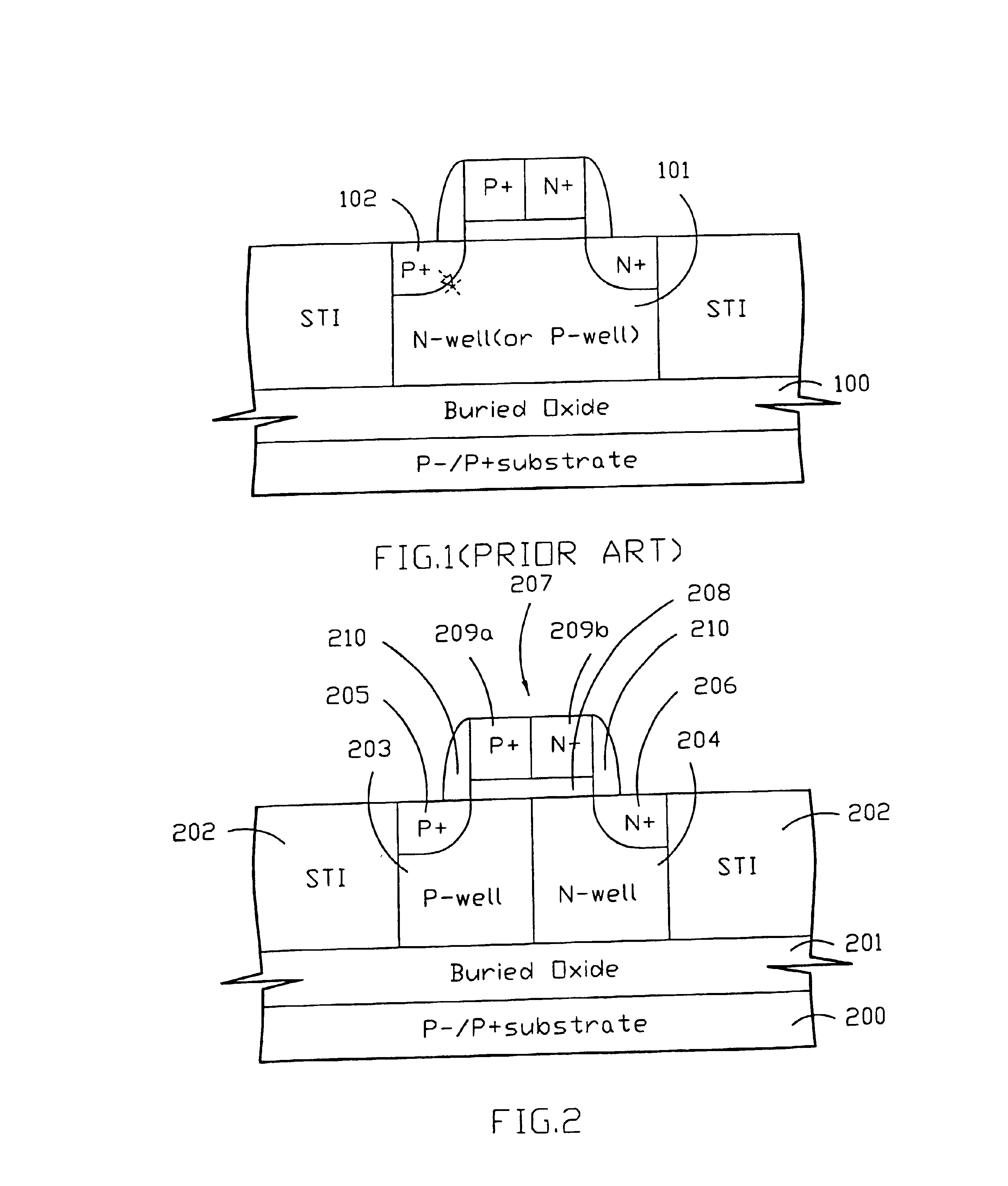
FIG. 2 is a cross-sectional view of a gated diode according to the present invention. The structure of FIG. 2 comprises a substrate 200, for example, a P− substrate or P+ substrate, and an insulating layer 201, such as a buried silicon dioxide layer, formed thereon. Two shallow trench isolations 202 are formed on the insulating layer 201, and a P-well 203 based on a silicon layer and an N-well 204 based on a silicon layer are formed on the insulating layer 201 between the two shallow trench isolations 202. The P-well 203 and the N-well 204 constitute a PN junction. A first highly doped P+ diffusion region 205 is formed at the upper corner of the P-well 203 adjacent to the one shallow trench isolation 202, and a second highly doped N+ diffusion region 206 is formed at the upper corner of N-well 204 adjacent to the other shallow trench isolation 202. A MOS-like gate 207 is formed on the P-well 203 and the N well 204, and the junction of the P well 203 and the N-well 204 is at the midd...


PUM


Abstract

A silicon-on-insulator (SOI) gated diode and non-gated junction diode are provided. The SOI gated diode has a PN junction at the middle region under the gate, which has more junction area than a normal diode. The SOI non-gated junction diode has a PN junction at the middle region thereof, and also has more junction area than a normal diode. The SOI diodes of the present invention improve the protection level offered for electrical overstress (EOS)/electrostatic discharge (ESD) due to the low power density and heating for providing more junction area than normal ones. The I/O ESD protection circuits, which comprise primary diodes, a first plurality of diodes, and a second plurality of diodes, all of which are formed of the present SOI diodes, could effectively discharge the current when there is an ESD event. And the ESD protection circuits, which comprise more primary diodes, could effectively reduce the parasitic input capacitance, so that they can be used in the RF circuits or HF circuits. The proposed gated diode and non-gated diode can be fully process-compatiable to general partially-depleted or fully-depleted silicon-on-insulator CMOS processes.

Description

BACKGROUND OF THE INVENTION1. Field of the InventionThe present invention relates to diodes in a silicon-on-insulator (SOI) CMOS process, and more particularly to ESD protection circuits with the diodes in a silicon-on-insulator CMOS process.2. Description of the Prior ArtSilicon-on-insulator technology is a prime contender for low-voltage, high-speed applications because of its advantages over bulk-Si technology in reduced process complexity, latch-up immunity and smaller junction capacitance. However, electrostatic discharge (ESD) is a major reliability concern for SOI technology.The protection level provided by an ESD protection device is determined by the amount of current that it can sink. The device failure is initiated by thermal runaway and is followed by catastrophic damage during an ESD pulse. In SOI devices, the presence of the buried oxide layer having a thermal conductivity {fraction (1 / 100)}th of Si causes increased device heating, which in turn accelerates thermal run...

Claims


Application Information

Patent Timeline
Patent Type & Authority Patents(United States)
IPC IPC(8): H01L29/66H01L29/739H01L27/02H01L29/861
CPCH01L27/0251H01L29/861H01L29/7391H01L29/4983H01L29/4991
Inventor KER, MING-DOUHUNG, KEI-KANGTANG, TIEN-HAO
Owner UNITED MICROELECTRONICS CORP
Why Eureka
Try Eureka