

Memory device
a memory device and memory technology, applied in the field of new memory devices, can solve the problems of increasing start-up times, complicated data storage, and substantial complexity of computer system operation, and achieve the effects of improving memory storage and retrieval
- Summary
- Abstract
- Description
- Claims
- Application Information
AI Technical Summary
Benefits of technology
Problems solved by technology
Method used
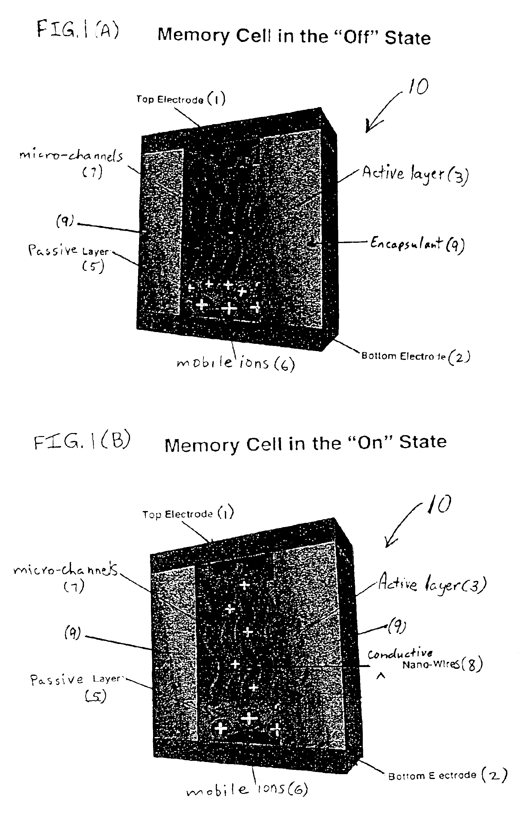
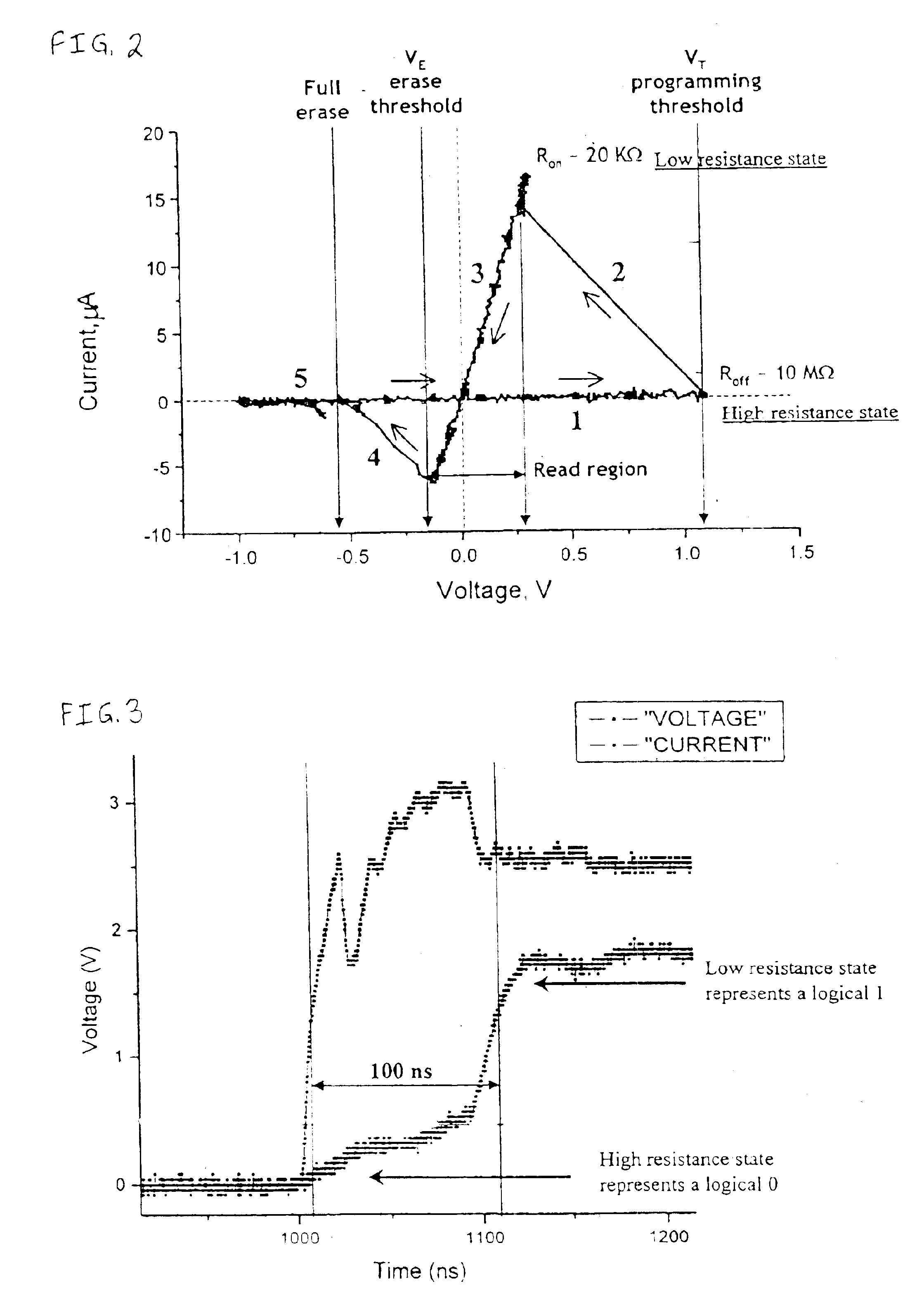
Image

Examples
example 1
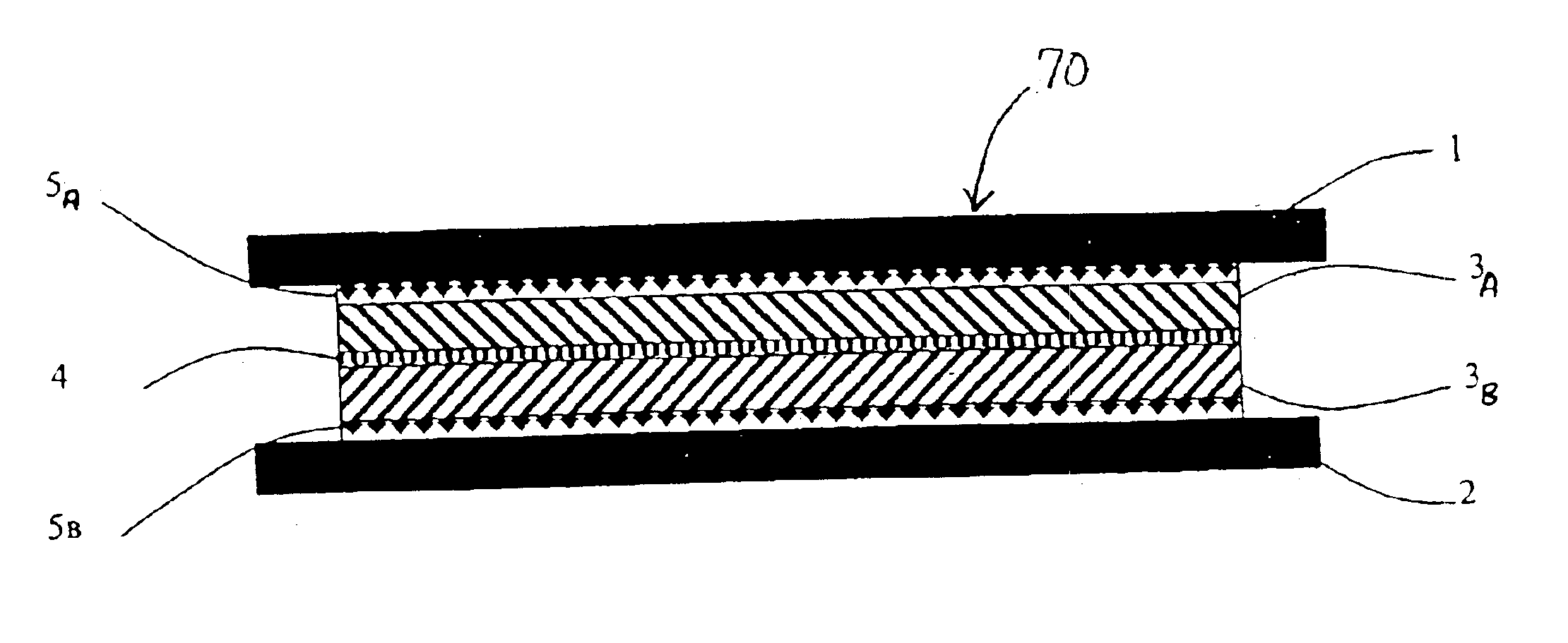
Ti / LixVSe2 / Al (or Ti), wherein LixVSe2 serves as a combined active+passive layer (as in FIG. 4). The first, or lower electrode of Ti or Al was vapor deposited on the surface of an insulating layer at a thickness of about 3,000-8,000 Å, preferably about 5,000 Å. The LixVSe2 combined active+passive layer was deposited via CVD at a thickness of about 50-300 Å, preferably about 100 Å, with Li ions intercalated by treatment with a solution of n-butyl lithium in hexane. The second, or upper electrode of Ti or Al was vapor deposited on the LixVSe2 layer at a thickness of about 3,000-8,000 Å, preferably about 5,000 Å.
example 2
Ti / LixTiS2 / VSe2 / Al (or Ti), wherein LixTiS2 serves as a passive layer and VSe2 serves as an active layer (as in FIG. 5). This cell was fabricated in similar manner as Example 1, except that the VSe2 active layer was deposited by CVD on the surface of the LixTiS2 passive layer prior to deposition of the second, upper electrode. The thickness of the VSe2 active layer was about 50-300 Å, preferably 100 Å.
example 3
Ti / LixVSe2 / HfSe2 / Al (or Ti), wherein LixVSe2 serves as a passive layer and HfSe2 serves as an active layer, each layer being deposited via CVD.
PUM
| Property | Measurement | Unit |
|---|---|---|
| temperatures | aaaaa | aaaaa |
| temperatures | aaaaa | aaaaa |
| programming threshold voltage VT | aaaaa | aaaaa |
Abstract
Description
Claims
Application Information