Programmable logic device

a logic device and programmable logic technology, applied in the direction of instruments, computation using denominational number representation, pulse technique, etc., can solve the problem of general limited fifo depth

Inactive Publication Date: 2005-03-08
MONTEREY RES LLC
View PDF31 Cites 119 Cited by
  • Summary
  • Abstract
  • Description
  • Claims
  • Application Information

AI Technical Summary

Problems solved by technology

However, the depth of the FIFO will generally

Method used


Image

  • Programmable logic device
  • Programmable logic device
  • Programmable logic device

Examples


Embodiment Construction

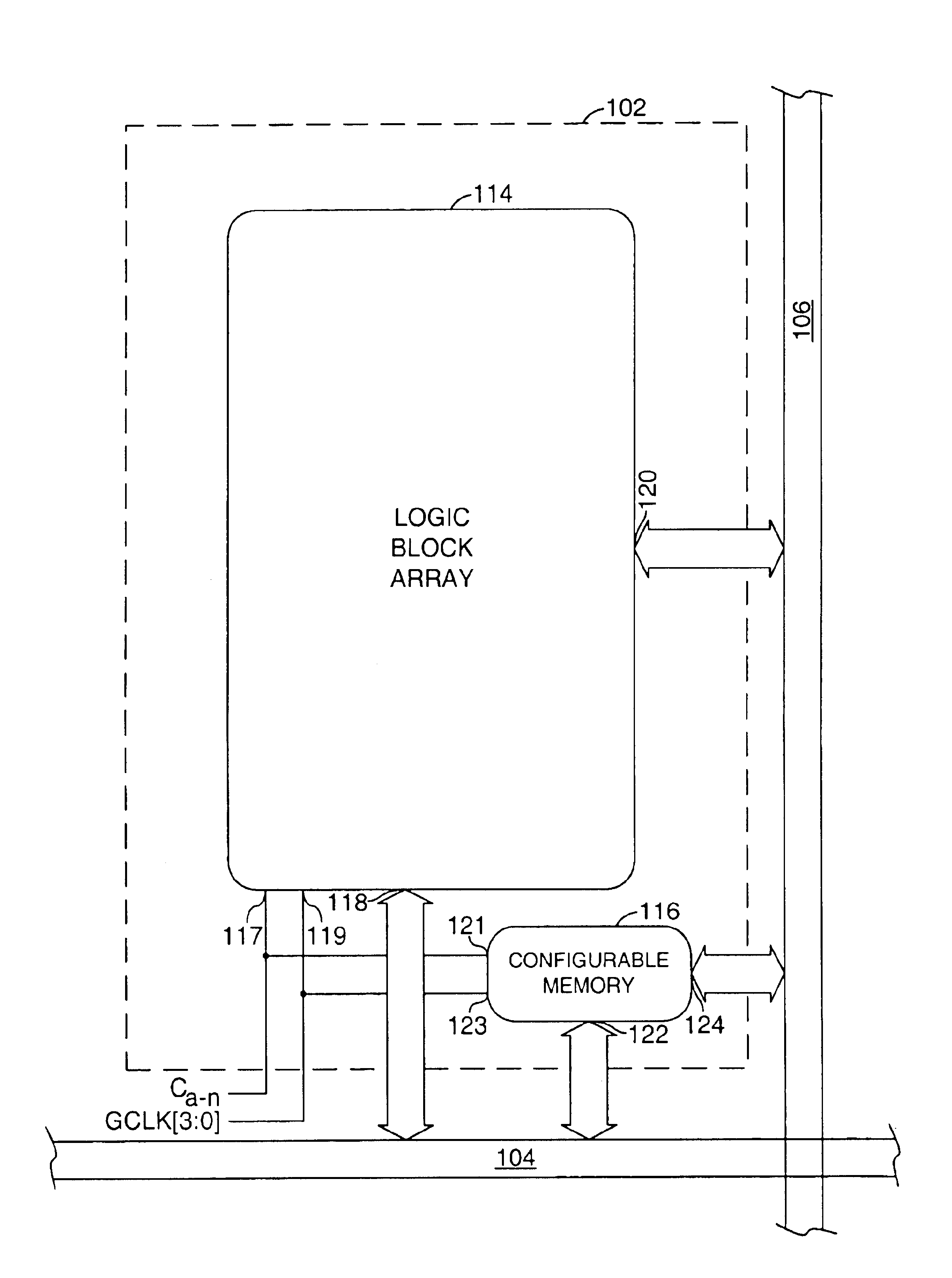
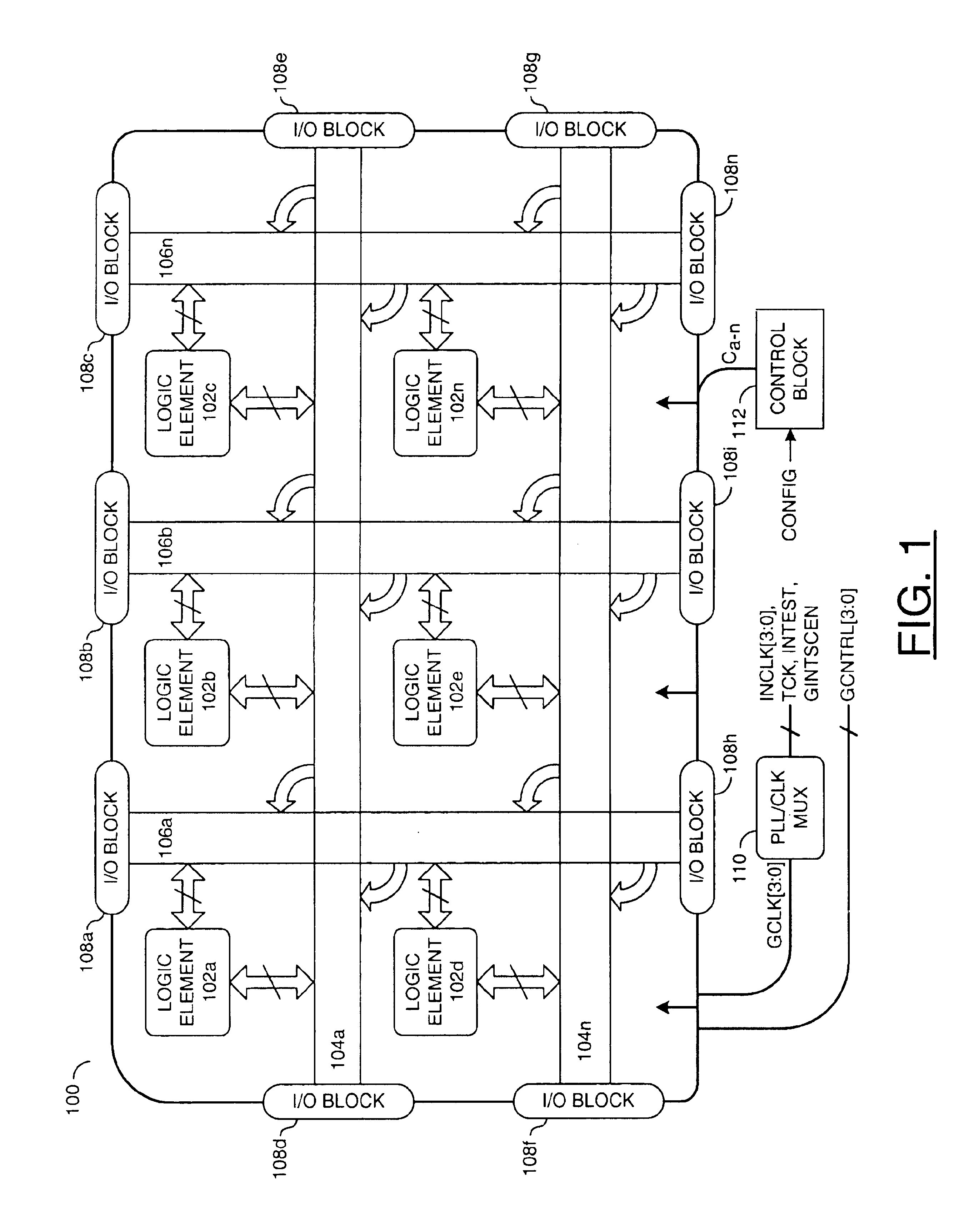
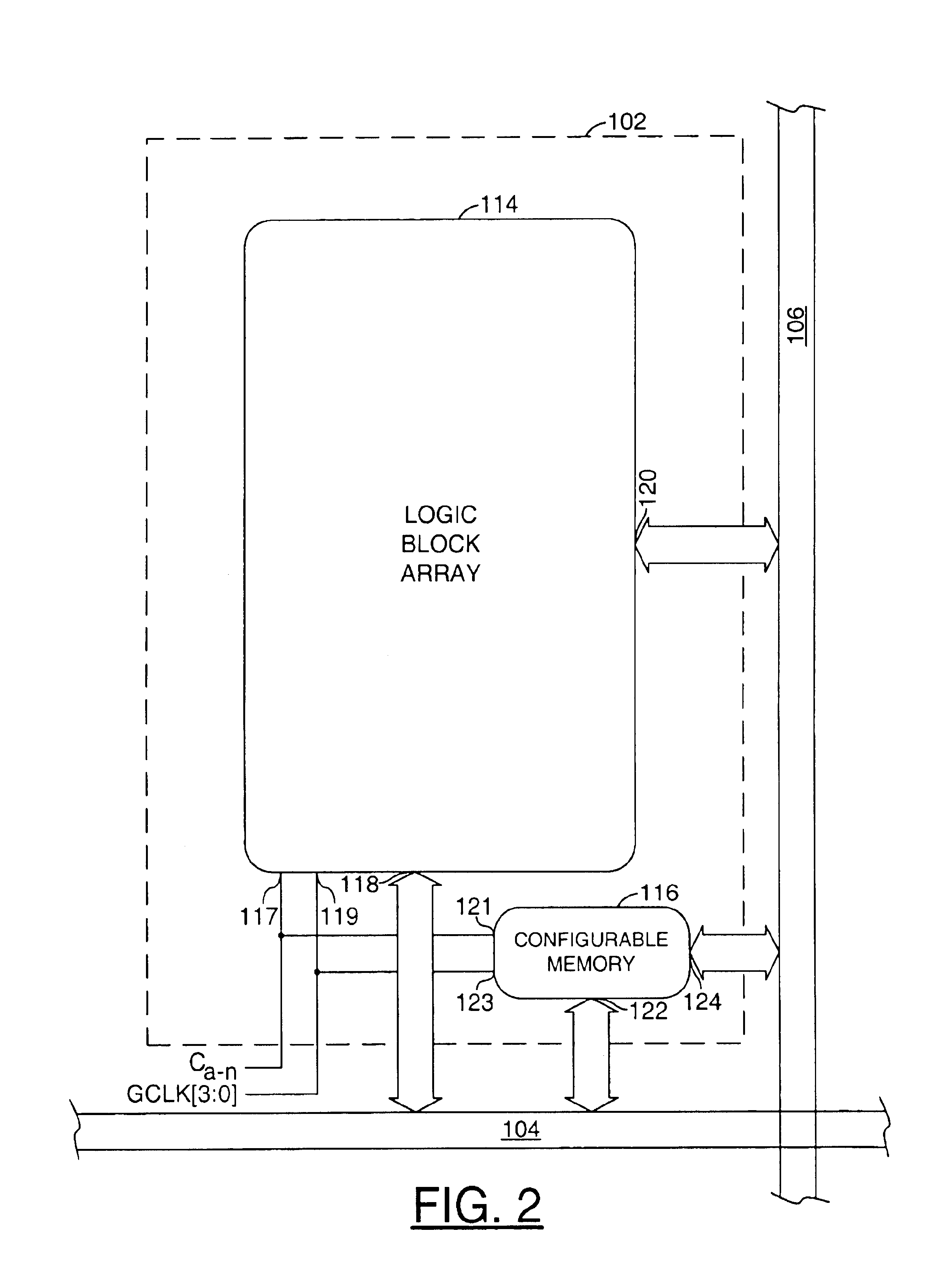
Referring to FIG. 1, a block diagram of a programmable logic device (PLD) 100 is shown in accordance with a preferred embodiment of the present invention. The PLD 100 may be implemented using an advanced CMOS logic process. The PLD 100 may be implemented as a volatile or non-volatile device. When a non-volatile device is desired, the PLD 100 may be implemented with a separate non-volatile storage device within the same package. The PLD 100 may support, in one example, an external core voltage of 3.3V, 2.5V, or 1.8V through the use of an internal voltage regulator. The range of core voltages may provide for the migration of previous applications to the PLD 100 without requiring a change in a power supply scheme.

The PLD 100 may comprise, in one example, a number of logic elements 102a-102n, a number of horizontal routing channels 104a-104n, a number of vertical routing channels 106a-106n, a number of I / O blocks 108a-108n, a PLL / CLK multiplexer circuit 110, and a control circuit 112. T...


PUM


Abstract

A programmable logic device comprising one or more horizontal routing channels, one or more vertical routing channels, and a logic element. Each logic element may be configured to connect between one of the horizontal routing channels and one of the vertical routing channels. The logic element may comprise a logic block cluster and a memory block.

Description

FIELD OF THE INVENTIONThe present invention relates to programmable logic at devices generally and, more particularly, to a programmable logic device architecture that may combine the high-speed, predictable timing, and ease of use of a complex programmable logic device (CPLD) with the high density and low power of a field programmable so gate array (FPGA).BACKGROUND OF THE INVENTIONTraditionally there are two types of programmable logic architectures: complex programmable logic device (CPLDs) and field programmable gate arrays (FPGAs). The CPLD can be constructed as a one-dimensional array of logic blocks made of 16 macrocells and a product term array connected through a single central interconnect scheme. The CPLD achieves high performance by being able to complete a complex logic function in a single-pass of the logic array and has predictable timing by having every output or I / O pin connected to every logic block input through the central interconnect structure. The CPLD can be ...

Claims


Application Information

Patent Timeline
IPC IPC(8): H03K19/177
CPCH03K19/17728H03K19/17796H03K19/17744H03K19/17736
Inventor LACEY, TIMOTHY M.JOHNSON, DAVID L.
Owner MONTEREY RES LLC
Why Eureka
Try Eureka