

Exposure process and exposure device
a technology of exposure process and exposure device, which is applied in the field of exposure process, can solve the problems of degrading the visual detectability of alignment marks, affecting the detection accuracy of alignment marks, so as to achieve the effect of difficult determination of alignment marks
- Summary
- Abstract
- Description
- Claims
- Application Information
AI Technical Summary
Benefits of technology
Problems solved by technology
Method used
Image

Examples
first embodiment
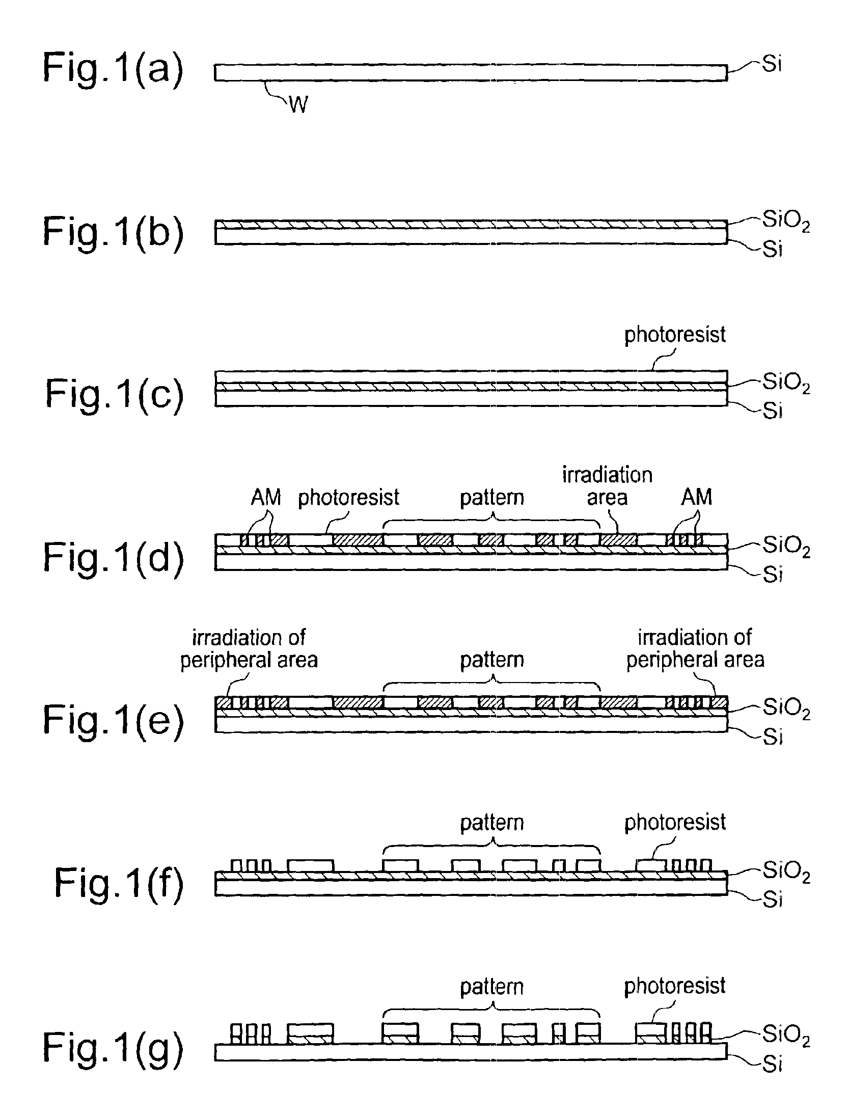
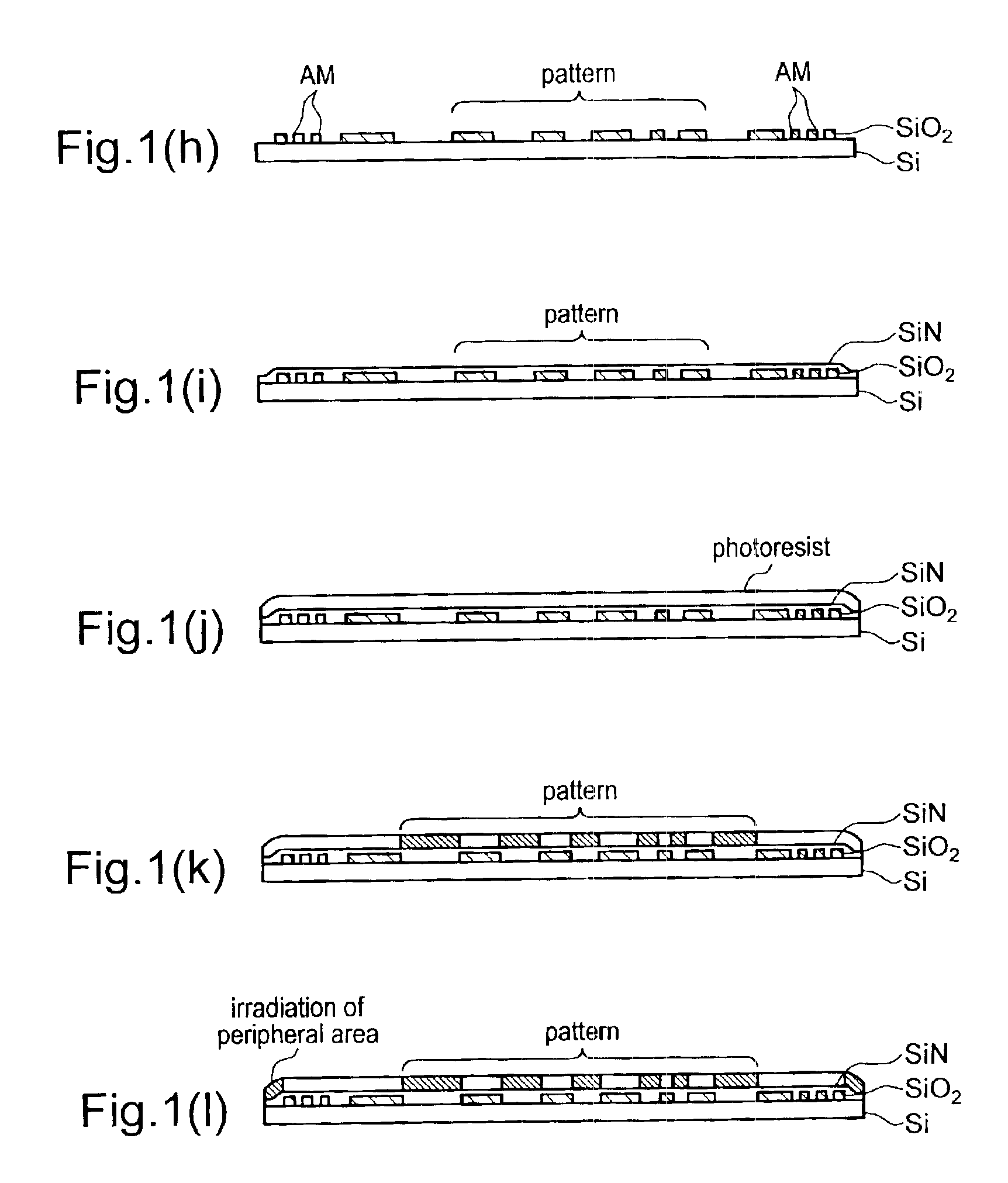
First, the process of pattern formation in accordance with the invention will be described using FIGS. 1(a) to 1(p) and using the process flow chart shown in FIG. 2. In the embodiment described below, a wafer is described which has a notch. However, the invention can also be applied to a wafer which has an orientation flat, and to an angular substrate.
(1) A film, such as an oxide film (SiO2), a nitride film (SiN) or the like is formed on a Si substrate (a wafer) which is shown in FIG. 1(a), by thermal oxidation, by CVD or the like, as is shown in FIG. 1(b) (step S1 in FIG. 2). In this example, a silicon oxide film (SiO2) is formed.
(2) As shown in FIG. 1(c), the resist is applied (step S2 in FIG. 2). By a stepper or the like, an element pattern and alignment marks AM are exposed, as is shown in FIG. 1(d) (step S3 in FIG. 2). In FIG. 1(d) the exact arrangement of the element pattern is not shown.
(3) As shown in FIG. 1(e), peripheral area exposure is performed in order to eliminate unn...
third embodiment
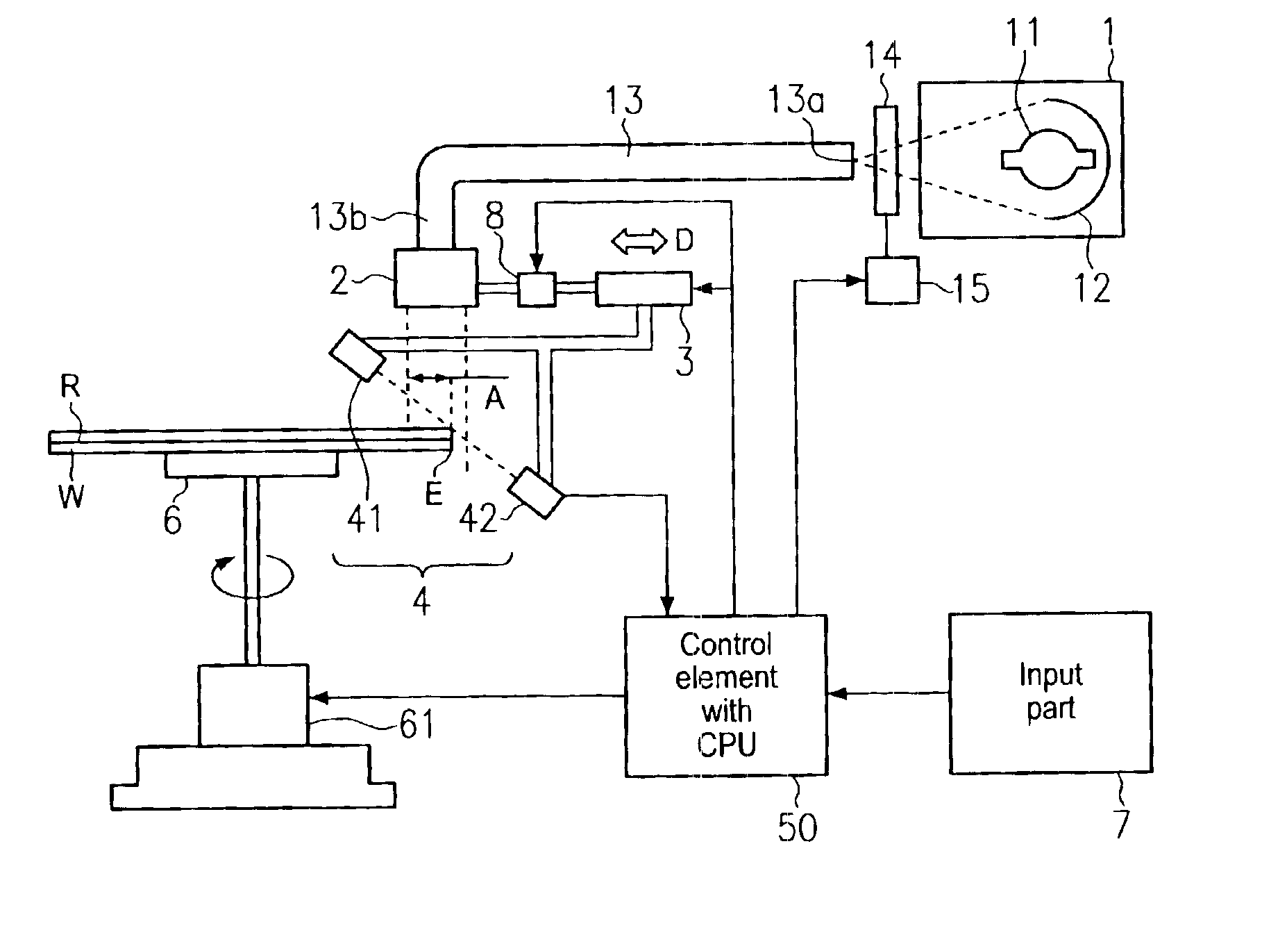
FIG. 9 shows the arrangement of an exposure device according to the invention. In the exposure device in this embodiment, the invention is used for an exposure device in which the peripheral area of the wafer is gradually exposed by moving the exposure light outlet part 2 in the X-Y directions.
In FIG. 9, a light source part I has a lamp 11 which emits light which contains UV radiation, such as a super-high pressure mercury lamp or the like. The radiant light from this lamp 11 is focused by means of a focusing mirror 12 on the incidence face side of optical fibers 13.
Between the lamp 11 and the incidence face side of the optical fibers 13, there is a shutter 14, as was described above. The shutter 14 is opened when a shutter opening signal is sent from the control element 51. In this way, exposure light with a given irradiation area S is emitted from the exposure light outlet part 2, as was described above.
The exposure light outlet part 2 is mounted in a device 20 for moving the irra...
PUM
| Property | Measurement | Unit |
|---|---|---|
| diameter | aaaaa | aaaaa |
| area | aaaaa | aaaaa |
| size | aaaaa | aaaaa |
Abstract
Description
Claims
Application Information