Semiconductor laser element

Active Publication Date: 2005-03-08
SHARP FUKUYAMA LASER CO LTD
View PDF14 Cites 18 Cited by
  • Summary
  • Abstract
  • Description
  • Claims
  • Application Information

AI Technical Summary

Problems solved by technology

However, the above-mentioned semiconductor laser element has the problem that the rise time and the fall time of the output become comparatively long and the pulse waveform becomes dull when the pulse oscillation is effected with a high output.
This dullness of the pulse waveform deteriorates the quality of a signal to be written in an

Method used


Image

  • Semiconductor laser element
  • Semiconductor laser element
  • Semiconductor laser element

Examples


Example

(First Embodiment)

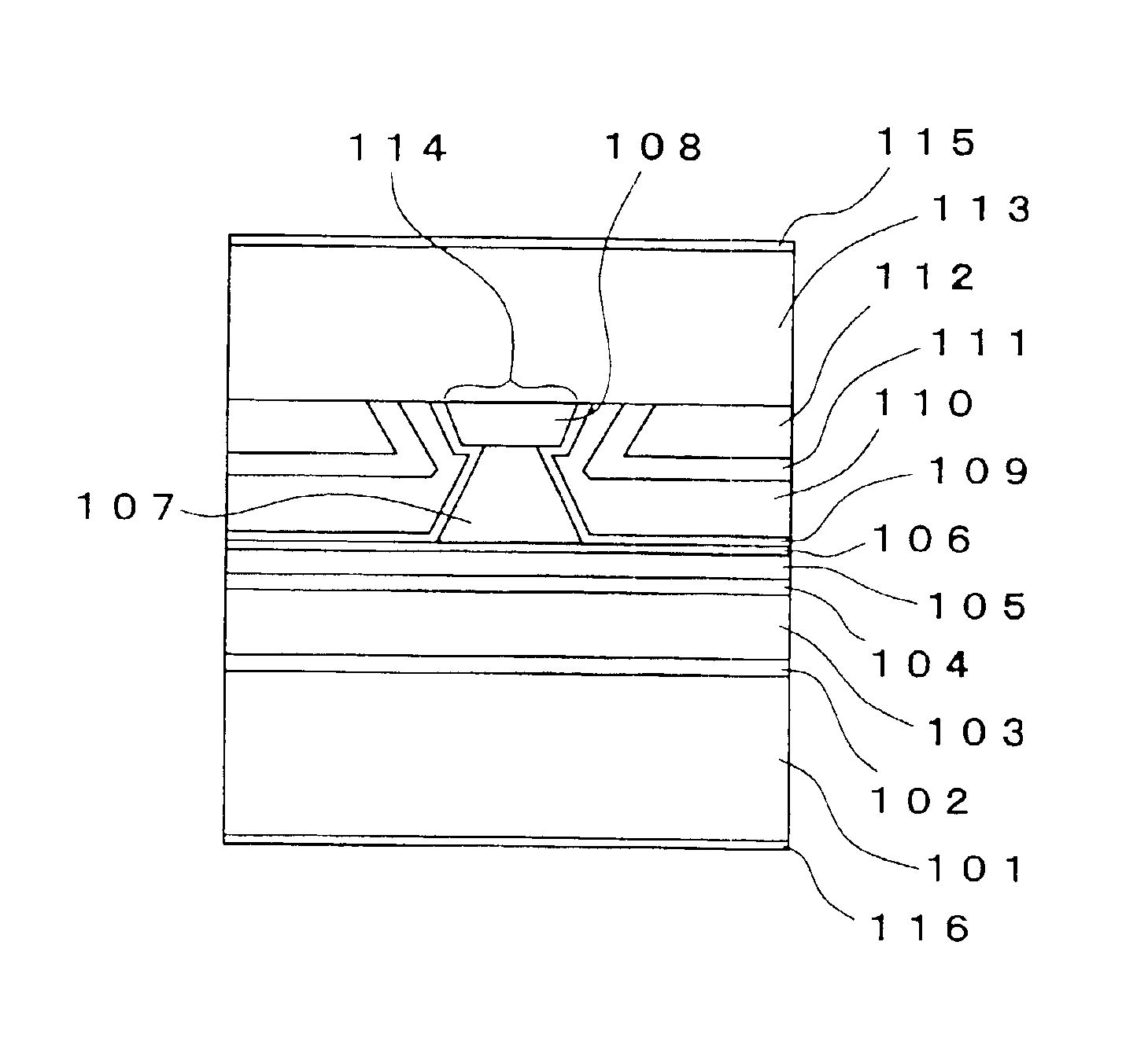
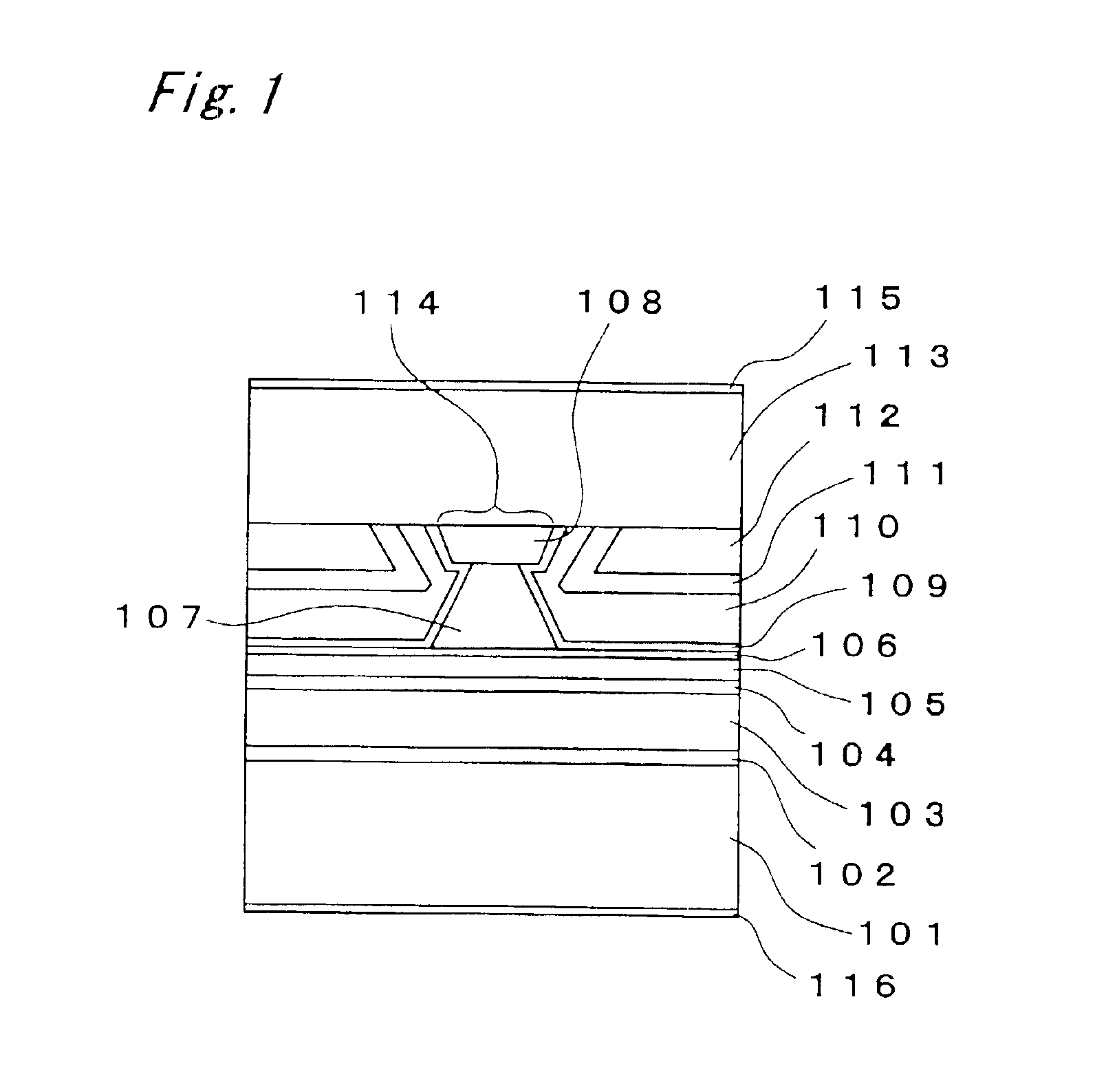
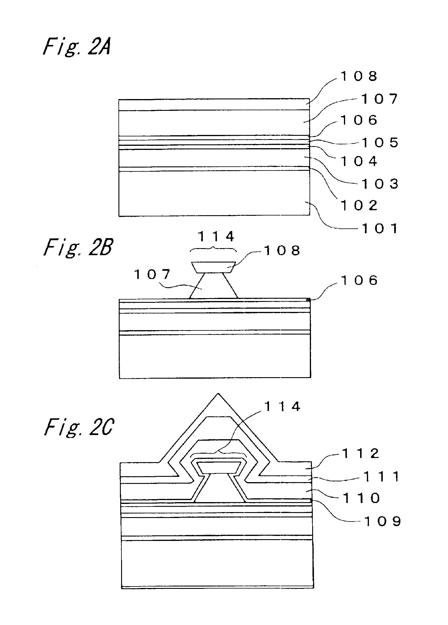
FIG. 1 is a view showing the semiconductor laser element of the first embodiment of the present invention. In this semiconductor laser element, an n-type GaAs buffer layer 102, an n-type Al0.5Ga0.5As first clad layer 103, an MQW active layer 104, a p-type Al0.5Ga0.5As second clad layer 105 and a p-type GaAs etching stop layer 106 are successively laminated on an n-type GaAs substrate 101. A ridge-shaped p-type Al0.5Ga0.5As third clad layer 107 and a p-type GaAs protective layer 108 are provided on this etching stop layer 106. The ridge-shaped p-type Al0.5Ga0.5As third clad layer 107 and the p-type GaAs protective layer 108 constitute a ridge portion 114 extended in the direction of a resonator. A p-type Al0.7Ga0.3As spacer layer 109 is provided on both sides in the widthwise direction of this ridge portion 114. An n-type Al0.7Ga0.3As current light confining layer 110, an n-type GaAs current confining layer 111 and a p-type GaAs flattening layer 112 are laminated on...

Example

(Second Embodiment)

FIG. 5 is a view showing the semiconductor laser element of the second embodiment of the present invention. This semiconductor laser element differs from the semiconductor laser element of the first embodiment only in the carrier density of the substrate, the layer thickness of the second clad layer, the impurity contained mainly in this second clad layer, the impurity contained mainly in the etching stop layer, the dopant, layer thickness and carrier density of the spacer layer, the carrier density of the current light confining layer and the layer thickness of the current confining layer. The same portions as those of the semiconductor laser element of the first embodiment are denoted by same reference numerals, and no detailed description is provided therefor.

In the semiconductor laser element of the present embodiment, an n-type GaAs substrate 201 has a carrier density of 1×1018 cm−3. A p-type Al0.5Ga0.5As second clad layer 205 has a layer thickness of 0.1 μm....

Example

(Third Embodiment)

FIG. 6 is a view showing the semiconductor laser element of the third embodiment of the present invention. In this semiconductor laser element, an n-type GaAs buffer layer 302, an n-type (Al0.7Ga0.3)InP first clad layer 303, an MQW active layer 304 and a p-type (Al0.7Ga0.3)InP second clad is layer 305 are successively laminated on an n-type GaAs substrate 301. A p-type GaInP etching stop layer 306 is formed to have a predetermined width at the center in the widthwise direction on this p-type second clad layer 305. A ridge-shaped p-type (Al0.7Ga0.3)InP third clad layer 307 and a p-type GaAs protective layer 308 are provided on this etching stop layer 306. The etching stop layer 306, the third clad layer 307 and the protective layer 308 constitute a ridge portion 314 extended in the direction of resonator. A p-type AlInP spacer layer 309 is provided on both sides in the widthwise direction of this ridge portion 314. An n-type AlInP current light confining layer 310, ...


PUM


Abstract

There is provided a semiconductor laser element, which has a small capacitance outside a ridge portion and high response speed and is able to effect pulse oscillation with a satisfactory pulse waveform. On a GaAs substrate 101, there are provided an n-type buffer layer 102, an n-type first clad layer 103, an MQW active layer 104, a p-type second clad layer 105, a p-type etching stop layer 106 that has an energy bandgap smaller than that of this second clad layer 105, a p-type third clad layer 107 that constitutes a ridge portion and a p-type protective layer 108. On both sides in the widthwise direction of the ridge portion are laminated a p-type spacer layer 109, an n-type current light confining layer 110, an n-type current confining layer 111 and a p-type flattening layer 112. On these layers is laminated a p-type contact layer 113. A depletion layer spreads into the spacer layer 109 when a bias voltage is applied. Therefore, a capacitance between the spacer layer 109 and the current light confining layer 110 is reduced, and a response speed during the pulse oscillation of the semiconductor laser element becomes fast.

Description

BACKGROUND OF THE INVENTIONThe present invention relates to a semiconductor laser element.Conventionally, there has been a semiconductor laser element as shown in FIG. 10 (refer to Japanese Patent Laid-Open Publication No. HEI 9-199790). This semiconductor laser element is a semiconductor laser element of an effective refractive index waveguide type. On an n-type GaAs substrate 501, there are provided an n-type GaAs buffer layer 502, an n-type AlGaAs first clad layer 503, a quantum well active layer 504, a p-type AlGaAs second clad layer 505, a p-type GaAs etching stop layer 506, a p-type AlGaAs third clad layer 507 and a p-type GaAs cap layer 508. The p-type AlGaAs third clad layer 507 and the p-type GaAs cap layer 508 are formed in a ridge-like shape to constitute a ridge portion 513. An n-type AlGaAs current light confining layer 509, an n-type GaAs current confining layer 510 and a p-type GaAs flattening layer 511 are laminated on both sides in the widthwise direction of this ri...

Claims


Application Information

Patent Timeline
IPC IPC(8): H01S5/223H01S5/00H01S5/20H01S5/22H01S5/34H01S5/343
CPCH01S5/2231H01S5/2004H01S5/222H01S5/34
Inventor MATSUMOTO, MITSUHIRO
Owner SHARP FUKUYAMA LASER CO LTD
Why Eureka
Try Eureka