Semiconductor laser light emitting device

a semiconductor laser and light-emitting device technology, applied in semiconductor lasers, laser details, electrical equipment, etc., can solve problems such as deteriorating the performance of semiconductor laser light-emitting devices, and achieve the effects of low laser noise, low current drive, and reduced drive curren

Inactive Publication Date: 2005-03-08
SONY CORP
View PDF4 Cites 19 Cited by
  • Summary
  • Abstract
  • Description
  • Claims
  • Application Information

AI Technical Summary

Benefits of technology

[0033]In the third semiconductor laser light emitting device, since the component ratio “x” of Al is specified at a value in the range of 0≦x≦0.15, the light waveguide mechanism of the device becomes a gain guide type waveguide mechanism suitable for drive with low laser noise. Also, since the current injection width Wst of the current injection region is in the range of 1 μm≦Wst≦3 μm, a drive current is reduced, thereby enabling low current drive. Further, since part, present between an active layer and the current non-injection region, of the stacked film under the current non-injection region at least includes a film which is made from a material expressed by a chemical formula AlxGa1-xN (0≦x≦0.15) and which has a thickness of 0.2 μm or less, leak current can be suppressed. If the thickness of the above film made from AlxGa1-xN (0≦x≦0.15) is larger than 0.2 μm, leak current becomes larger, thereby deteriorating the performance of the semiconductor laser light emitting device.

Problems solved by technology

If the thickness of the above film made from AlxGa1-xN (0.3≦x≦1.0) is larger than 0.2 μm, leak current becomes larger, thereby deteriorating the performance of the semiconductor laser light emitting device.

Method used


Image

  • Semiconductor laser light emitting device
  • Semiconductor laser light emitting device
  • Semiconductor laser light emitting device

Examples


first embodiment

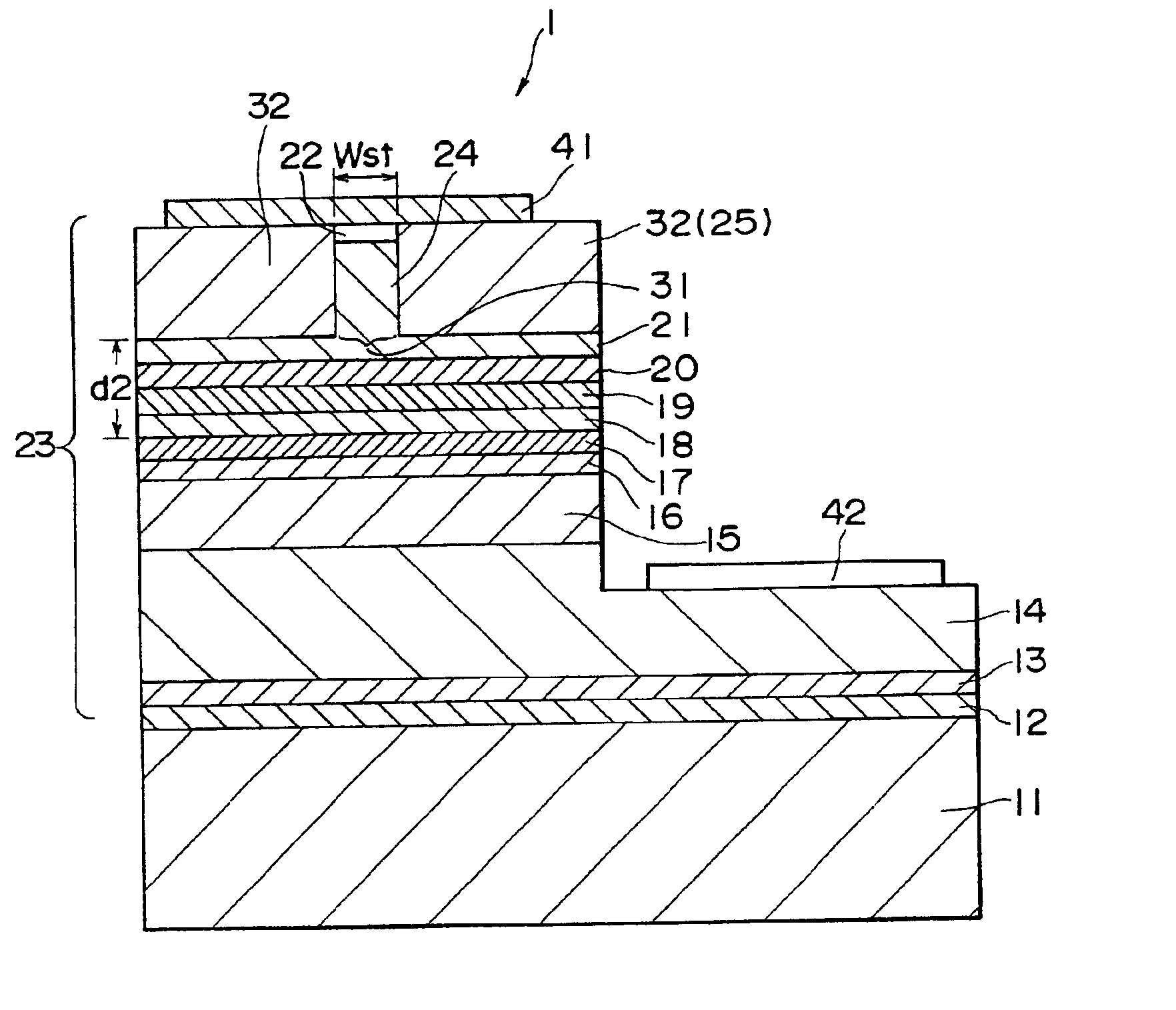
[0054]According to the present invention, the semiconductor laser light emitting device 1 shown in FIG. 1 is configured as an index guide type semiconductor laser light emitting device in which the current non-injection region 32 is made from the AlxGa1-xN layer 25, wherein the component ratio “x” of Al is specified at a value in a range of 0.3≦x≦1.0, which device is hereinafter referred to as “first semiconductor laser light emitting device”.

[0055]The first semiconductor laser light emitting device is further characterized as follows:

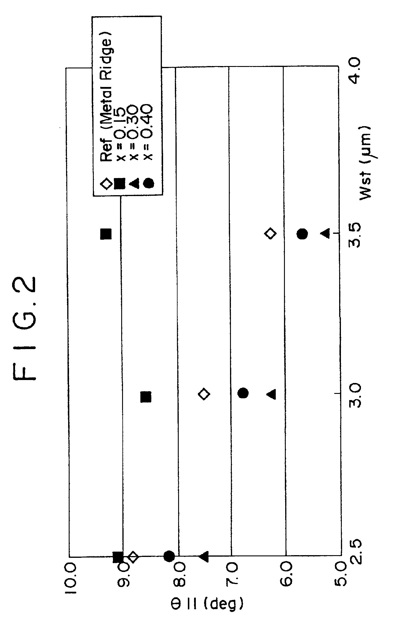
[0056](1) The current injection width Wst of the current injection region 31 formed into the ridge-like stripe is specified at a value in a range of 1 μm≦Wst≦3 μm.

[0057](2) Part, present between the active layer 17 and the current non-injection region 32, of the stacked film under the current non-injection region 32, that is, the films composed of the diffusion preventive layer 18, optical guide layer 19, carrier overflow suppressing layer 20, and clad...

second embodiment

[0059]According to the present invention, the semiconductor laser light emitting device 1 shown in FIG. 1 is configured as a weak index guide type semiconductor laser light emitting device in which the current non-injection region 32 is made from the AlxGa1-xN layer 25, wherein the component ratio “x” of Al is specified at a value in a range of 0.15

[0060]The second semiconductor laser light emitting device is further characterized as follows:

[0061](1) The current injection width Wst of the current injection region 31 formed into the ridge-like stripe is specified at a value in a range of 1 μm≦Wst≦3 μm.

[0062](2) Part, present between the active layer 17 and the current non-injection region 32, of the stacked film under the current non-injection region 32, that is, the films composed of the diffusion preventive layer 18, optical guide layer 19, carrier overflow suppressing layer 20, ...

third embodiment

[0064]According to the present invention, the semiconductor laser light emitting device 1 shown in FIG. 1 is configured as a gain guide type semiconductor laser light emitting device in which the current non-injection region 32 is made from the AlxGa1-xN layer 25, wherein the component ratio “x” of Al is specified at a value in a range of 0≦x≦0.15, which device is hereinafter referred to as “third semiconductor laser light emitting device”.

[0065]The third semiconductor laser light emitting device is further characterized as follows:

[0066](1) The current injection width Wst of the current injection region 31 formed into the ridge-like stripe is specified at a value in a range of 1 μm≦Wst≦3 μm.

[0067](2) Part, present between the active layer 17 and the current non-injection region 32, of the stacked film under the current non-injection region 32, that is, the films composed of the diffusion preventive layer 18, optical guide layer 19, carrier overflow suppressing layer 20, and claddin...


PUM


Abstract

Disclosed is a semiconductor laser light emitting device including: a stacked film composed of a stack of group III nitride semiconductor films each containing at least one kind selected from aluminum, gallium, indium, and boron; wherein an upper portion of the stacked film is formed into a ridge-like stripe, to form a current injection region; a current non-injection region formed on both sides of the ridge-like stripe; and at least part of the current non-injection region is made from a material expressed by a chemical formula AlxGa1-xN (0≦x≦1.0). In this device, the component ratio “x” of Al is specified at a value in a range of 0.3≦x≦1.0, so that the semiconductor laser light emitting device is configured as an index guide type semiconductor laser light emitting device; the component ratio “x” of Al is specified at a value in a range of 0.15<x<0.30, so that the semiconductor laser light emitting device is configured as a weak index type pulsation semiconductor laser light emitting device; or the component ratio “x” of Al is specified at a value in a range of 0≦x≦0.15, so that the semiconductor laser light emitting device is configured as a gain guide type laser light emitting device.

Description

RELATED APPLICATION DATA[0002]The present application claims priority to Japanese Application No. P2000-083368 filed Mar. 24, 2000, which application is incorporated herein by reference to the extent permitted by law.BACKGROUND OF THE INVENTION[0003]The present invention relates to a semiconductor laser light emitting device, and particularly to a semiconductor laser light emitting device including a stack of group III nitride semiconductor films.[0004]A semiconductor laser light emitting device of a type including a stack of semiconductor films made from group III nitrides each containing at least one kind selected from aluminum, gallium, indium, and boron (hereinafter, referred to as “group III nitride semiconductor light emitting device”) has been disposed as a useful component of various systems, and a system using such a semiconductor laser light emitting device as a light source is being realized.[0005]The group III nitride semiconductor laser light emitting device is inferior...

Claims


Application Information

Patent Timeline
Patent Type & Authority Patents(United States)
IPC IPC(8): H01S5/323H01S5/00H01S5/223H01S5/22H01S5/065H01S5/227H01S5/30H01S5/343
CPCH01S5/32341H01S5/221H01S5/2231H01S5/2218H01S5/30
Inventor YOSHIDA, HIROSHIABE, MISUZUOHARA, MAHOYAMAGUCHI, TAKASHINAKAJIMA, HIROSHI
Owner SONY CORP
Why Eureka
Try Eureka