Structure for connecting non-radiative dielectric waveguide and metal waveguide, millimeter wave transmitting/receiving module and millimeter wave transmitter/receiver

a technology of non-radiative dielectric waveguides and metal waveguides, which is applied in the direction of antenna connectors, electrical devices, antennas, etc., can solve the problems of not being able to meet the miniaturization of a millimeter wave integrated circuit, conventional connection structures are not suited for circuit boards, and the structure is not satisfactory with respect to keeping signal losses small, etc., to achieve the effect of low loss

Inactive Publication Date: 2005-03-15
KYOCERA CORP
View PDF7 Cites 251 Cited by
  • Summary
  • Abstract
  • Description
  • Claims
  • Application Information

AI Technical Summary

Benefits of technology

In view of the problems of the related art, it is an object of the invention to provide a smaller connection structure with which transmission in the millimeter wave band above 30 GHz is possible with low loss, and which can transmit and receive high-frequency wave signals as radio waves.
According to the invention, with this configuration, it is possible to obtain a millimeter wave transmitter / receiver for a millimeter wave radar module or the like, which amplitude-modulates and transmits / receives millimeter wave signals, and which has excellent transmission characteristics for millimeter wave signals, making it possible to increase the detection distance of the millimeter wave radar.

Problems solved by technology

However, when the dielectric strip of an NRD guide is provided with a taper-shaped end, as described above, to connect the dielectric strip to a metal waveguide, the length of this tapered portion has to be at least twice the wavelength of the high-frequency signal, so that there is the drawback that it is not suitable for the miniaturization of a millimeter wave integrated circuit.
On the other hand, the configuration shown in FIG. 19 is suitable for miniaturization, but for high-frequency signals in the millimeter waveband of at least 30 GHz, the transmission loss when using a microstrip line is large, so that this conventional connection structure is not suited for circuit boards in which the signal frequency is 30 GHz or higher.
However, with this configuration, signals tend to be reflected and leak at the portion connecting the dielectric strip and the portion of the portion of the parallel planar conductor corresponding to the dielectric strip, and this structure is not satisfactory with respect to keeping signal losses small.

Method used


Image

  • Structure for connecting non-radiative dielectric waveguide and metal waveguide, millimeter wave transmitting/receiving module and millimeter wave transmitter/receiver
  • Structure for connecting non-radiative dielectric waveguide and metal waveguide, millimeter wave transmitting/receiving module and millimeter wave transmitter/receiver
  • Structure for connecting non-radiative dielectric waveguide and metal waveguide, millimeter wave transmitting/receiving module and millimeter wave transmitter/receiver

Examples


working example 1

The following is a description of a working example of the invention.

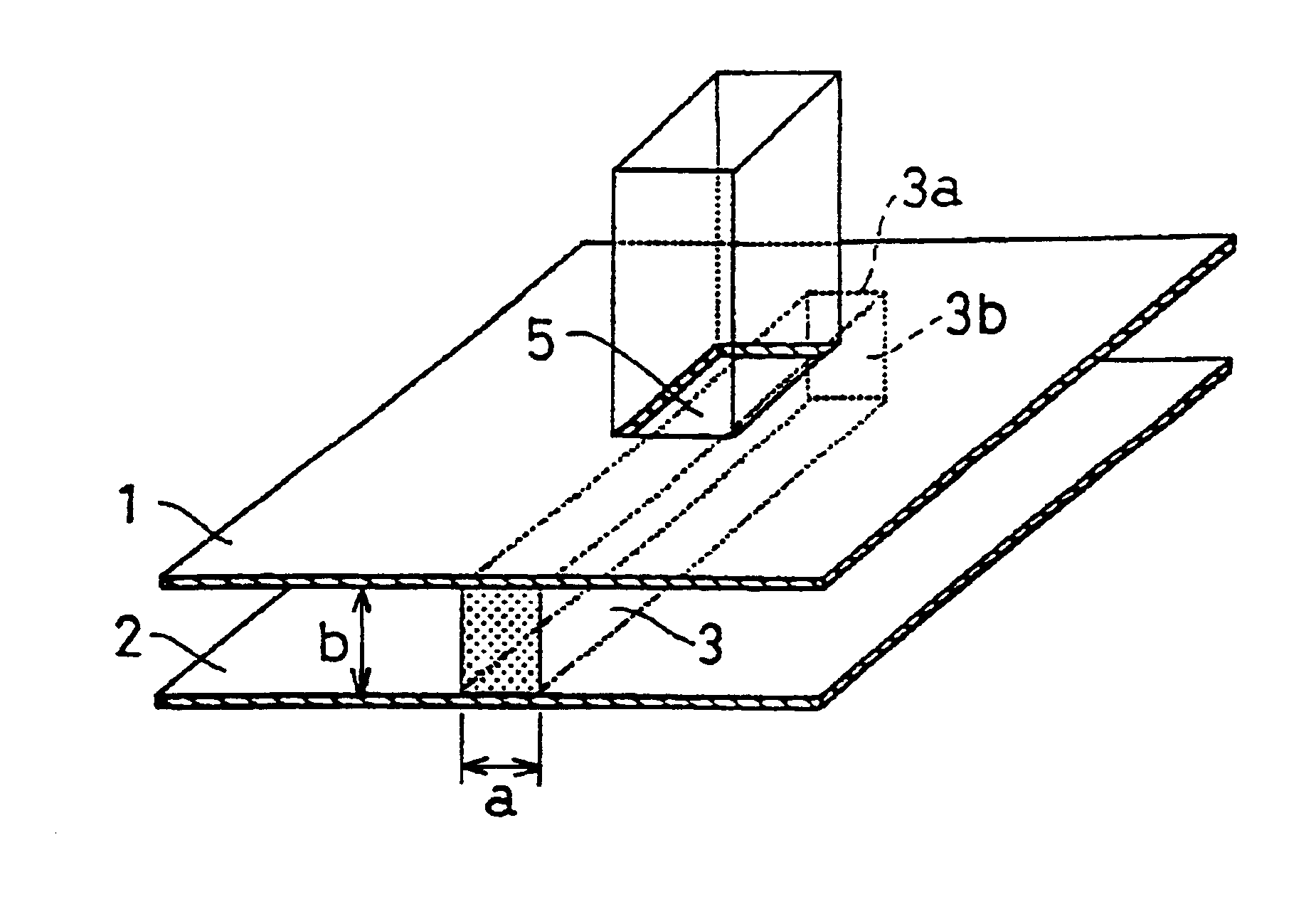
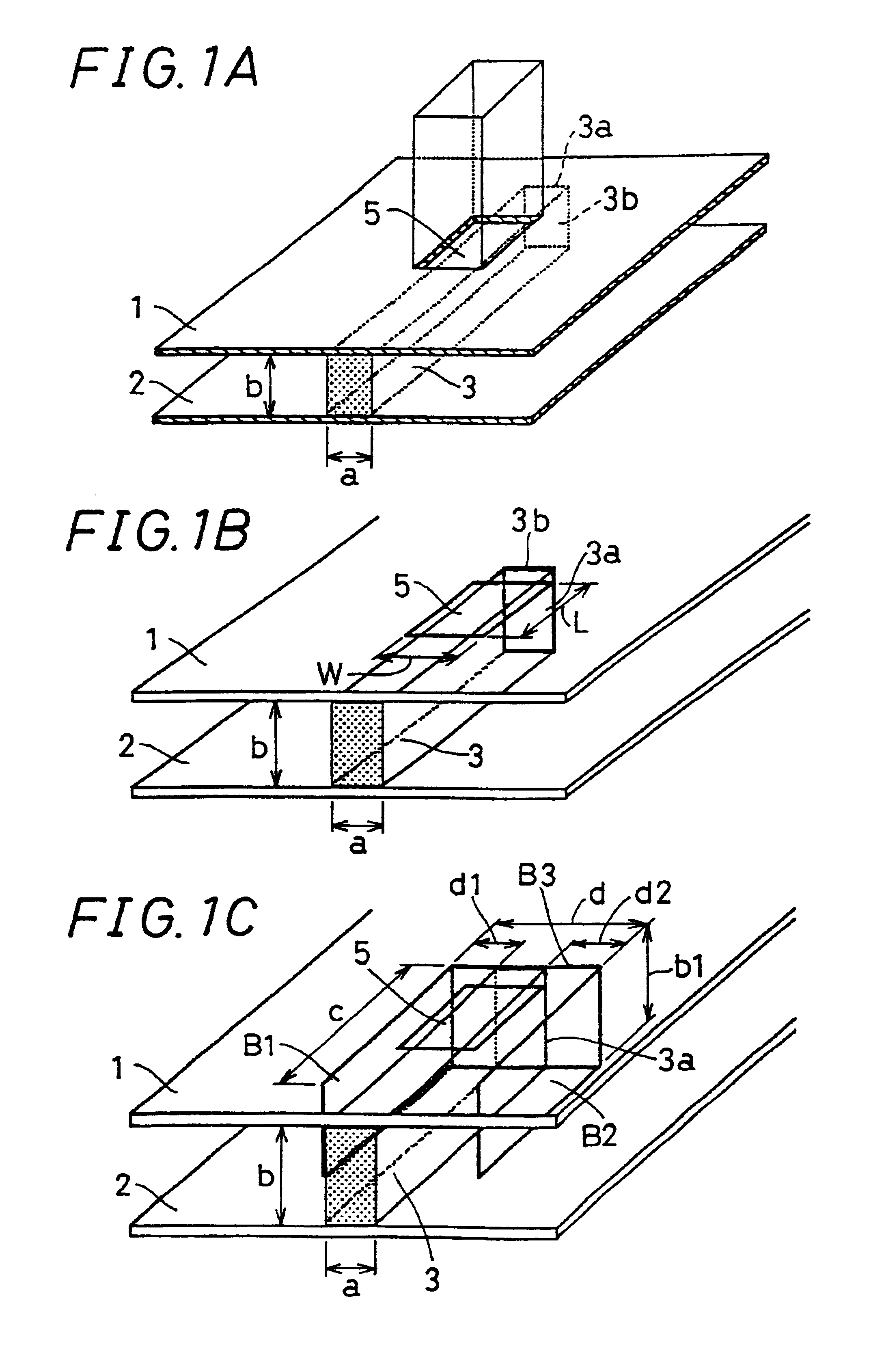
A structure for connecting an NRD guide and a metal waveguide as shown in FIGS. 1A to 1C and FIG. 4 was made as follows. First, the NRD guide of FIGS. 1A to 1C was prepared as follows: Two aluminum sheets of 6 mm thickness serving as the pair of parallel planar conductors 1, 2 were arranged in parallel at a distance of 1.8 mm, and a dielectric strip 3 made of cordierite ceramics with 0.8 mm width, 1.8 mm height, 60 mm length and a dielectric constant of 4.8 was placed between the parallel planar conductors 1, 2, thus producing the main portion of the NRD guide. Then, the connection structure shown in FIG. 1B was made on the side of the terminal end 3a of the dielectric strip 3. That is to say, centered on a position 3.2 mm from the end face of the terminal end 3a of the dielectric strip 3, a rectangular aperture 5 with a width W of 1.55 mm and a length L of 3.10 mm was formed in the parallel planar conductor 1.

Then...

working example 2

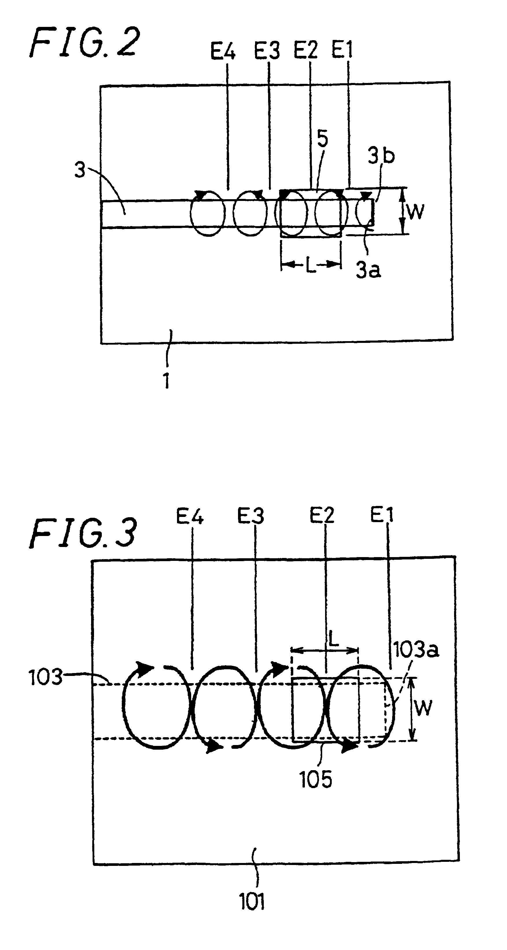
A structure for connecting an NRD guide and a metal waveguide as shown in FIGS. 11A and 11B and FIG. 12 was made as follows. First, the NRD guide of FIGS. 11A was prepared as follows: Two aluminum sheets of 6 mm thickness serving as the pair of parallel planar conductors 101, 102 were arranged in parallel at a distance of 1.8 mm, and a dielectric strip 103 made of cordierite ceramics with 0.8 mm width, 1.8 mm height, 60 mm length and a dielectric constant of 4.8 was placed between the parallel planar conductors 101, 102, thus producing the main portion of the NRD guide. Then, the connection structure shown in FIG. 11B was disposed on the top face of the main portion on the side of the terminal end 103a of the dielectric strip 103. That is to say, centered on a position 2.52 mm from the end face of the terminal end 103a of the dielectric strip 103, a rectangular aperture 105 with a width W of 1.55 mm and a length L of 3.10 mm was formed in the parallel planar conductor 101.

As shown i...


PUM


Abstract

It is an object of the invention to provide a connection structure for connecting the dielectric strip of an NRD guide with a metal waveguide, in which the conversion loss (connection loss) for high-frequency signals is reduced, and in which the NRD guide as well as the millimeter wave integrated circuit in which the NRD guide is incorporated can be made smaller. A non-radiative dielectric waveguide is made by arranging a dielectric strip for propagating high-frequency signals between parallel planar conductors arranged at a spacing of not more than half the wavelength of a high-frequency signal, a conductive member being arranged at an end face of a terminal end of the dielectric strip. An aperture is formed in at least one of the parallel planar conductors at a location where the electrical field of an LSM mode stationary wave propagating along the dielectric strip becomes largest. An open terminal end of a metal waveguide is connected to this aperture.

Description

BACKGROUND OF THE INVENTION1. Field of the InventionThe present invention relates to a structure for connecting a non-radiative dielectric waveguide and a metal waveguide, which is incorporated in, for example, a millimeter wave integrated circuit and used for the transmission of high frequency signals, and capable of transmitting and receiving high-frequency signals inform of radiowaves. The invention also relates to a millimeter wave transmitting / receiving module and a millimeter wave transmitter / receiver.2. Description of the Related ArtConventionally, non-radiative dielectric waveguides (also referred to as “NRD guides” in the following), in which a dielectric strip is sandwiched between a pair of parallel planar conductors, are known as one type of transmission line for high-frequency signals. When an NRD guide is incorporated on a printed circuit board or the like, the circuit has to be designed such that the NRD guide can be connected to other high-frequency transmission line...

Claims


Application Information

Patent Timeline
Patent Type & Authority Patents(United States)
IPC IPC(8): H01Q13/00H01Q13/06
CPCH01Q13/06H01R2201/02
Inventor HAYATA, KAZUKIMATSUI, KAZUHIROHIRAMATSU, NOBUKI
Owner KYOCERA CORP
Why Eureka
Try Eureka