

Method of varying optical properties of photonic crystals on fast time scales using energy pulses
- Summary
- Abstract
- Description
- Claims
- Application Information
AI Technical Summary
Benefits of technology
Problems solved by technology
Method used
Image

Examples
Embodiment Construction
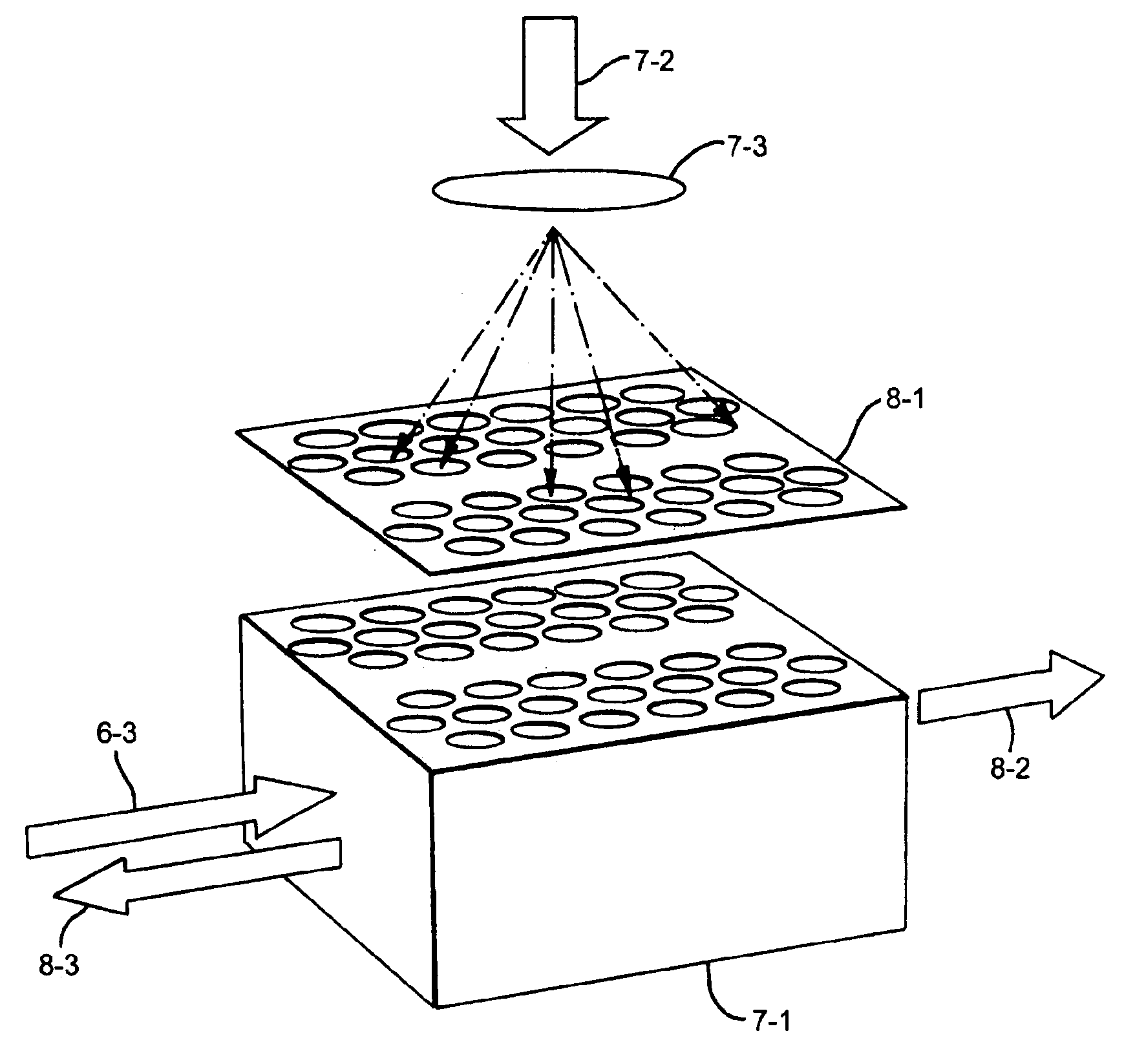
the crystal the incident light (6-3) might be either reflected back (8-3) or transmitted through the waveguide (8-2) depending on the waveguide pattern of free carriers generated in the crystal with the phase shift mask; and
[0033]FIG. 12 shows a pure / bulk semiconductor (7-1) where a 3D pattern of free carriers is optically generated via 4-wave mixing (8-1 to 8-4). On one side of the crystal the incident light (6-3) might be either reflected back (6-4) or transmitted through the photonic crystals (6-5) depending on the waveguide pattern of free carriers generated in the crystal with the phase shift mask.
DETEAILED DESCRIPTION OF THE INVENTION
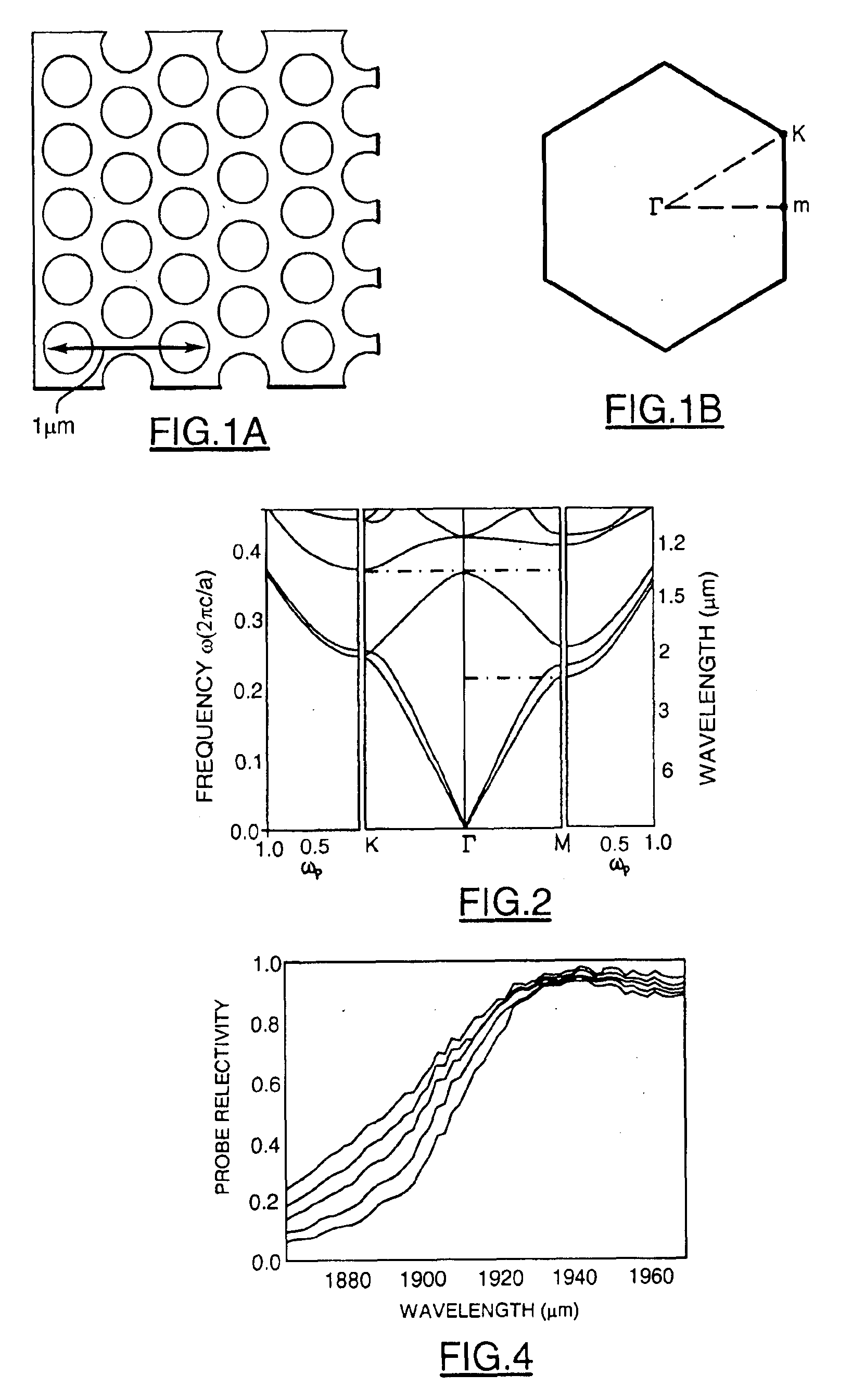
[0034]Broadly, the present invention provides a method for ultrafast, free carrier induced modulation of the optical properties of photonic crystals to provide control on time scales of optical properties of the photonic crystal such as bandgaps, stop-gaps, as well as dispersion curves associated with light waves outside the bandgap so that group ...
PUM
 Abstract
Description
Claims
Application Information