Method to use a laser to perform the edge clean operation on a semiconductor wafer

a technology of laser and semiconductor wafer, which is applied in the direction of cleaning using liquids, manufacturing tools, chemistry apparatus and processes, etc., can solve the problems of reducing the yield and loss of dies, peeling of edge films, and related defects of edges, so as to prevent slag buildup on other parts, accurate wafer alignment system, and accurate cleaning of the edge of the wafer

Inactive Publication Date: 2005-04-05
BELL SEMICON LLC
View PDF9 Cites 29 Cited by
  • Summary
  • Abstract
  • Description
  • Claims
  • Application Information

AI Technical Summary

Benefits of technology

An object of an embodiment of the invention is to provide a significant reduction in process steps necessary to accomplish the edge cleaning process on a semiconductor wafer.
An object of an embodiment of the invention is to provide for the elimination of the need for a very expensive resist coating track, photolithe stepper, plasma etcher, resist asher and solvent resist strip such that a significant reduction in capital equipment costs and a decrease in wafer cycle time are achieved.
Briefly, and in accordance with at least one of the foregoing, an embodiment of the present invention provides a method for performing the edge clean operation on a semiconductor wafer. Specifically, a laser beam is used to accurately clean the edge of the wafer. The wafer is clamped concentrically to a chuck and rotated at a selectable speed, such as in the range of 10 rpm to 1,000 rpm. A laser beam of variable power is directed onto the edge of the wafer at an oblique angle through a nozzle through which an inert purge gas is simultaneously passed. The laser beam removes unwanted deposits at the edge of the wafer and the gas is used to blow away the residue and prevent slag buildup on other parts of the wafer. The process is carried out in an exhausted chamber. Preferably, there is accurate wafer concentricity and laser alignment to the wafer edge. Preferably, an accurate form of wafer to chuck alignment system is used. This can be insured by use of a co-axial closed-loop video monitoring system that monitors both the edge of the wafer and the point of contact by the laser.

Problems solved by technology

One of the major problems gaining attention in wafer processing today is the edge related defects.
Edge related defects contribute to lower die yield and lost revenue.
A typical type of edge defect is the peeling of edge films due to poor adhesion to underlying layers.
The disadvantage associated with these existing solutions is that the wafers have to run through additional processing steps that can add both high cost and long cycle times.

Method used


Image

  • Method to use a laser to perform the edge clean operation on a semiconductor wafer
  • Method to use a laser to perform the edge clean operation on a semiconductor wafer
  • Method to use a laser to perform the edge clean operation on a semiconductor wafer

Examples


Embodiment Construction

While this invention may be susceptible to embodiment in different forms, there is shown in the drawings and will be described herein in detail, a specific embodiment with the understanding that the present disclosure is to be considered an exemplification of the principles of the invention, and is not intended to limit the invention to that as illustrated and described herein.

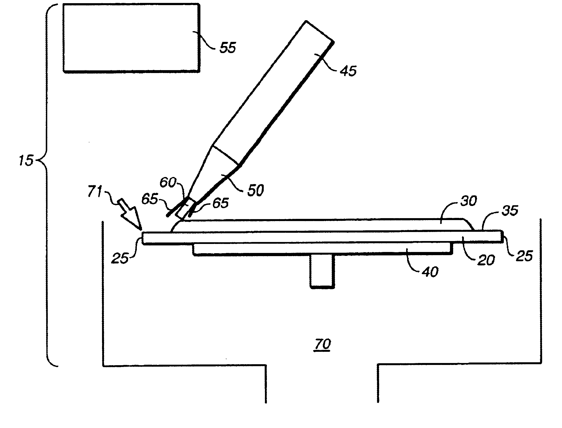
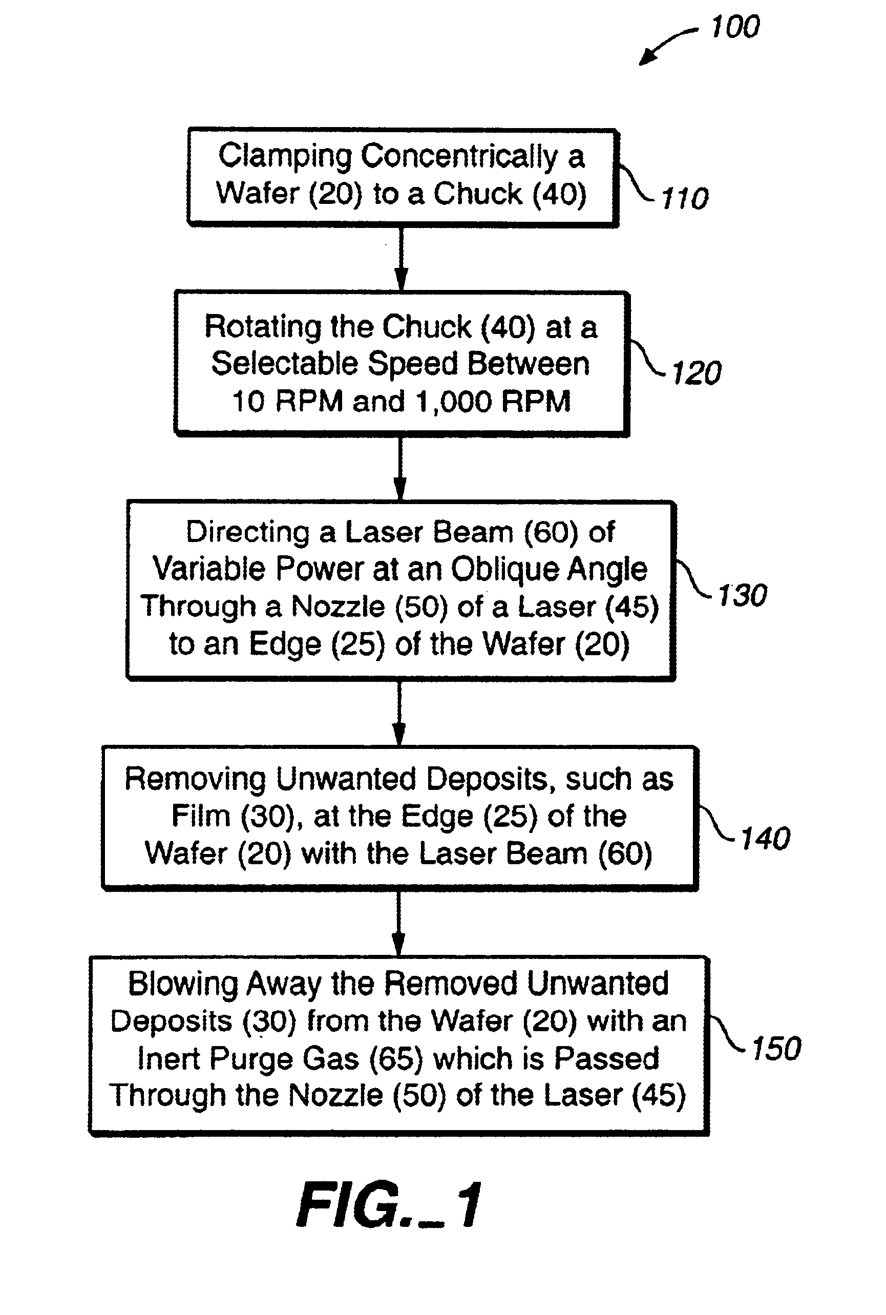
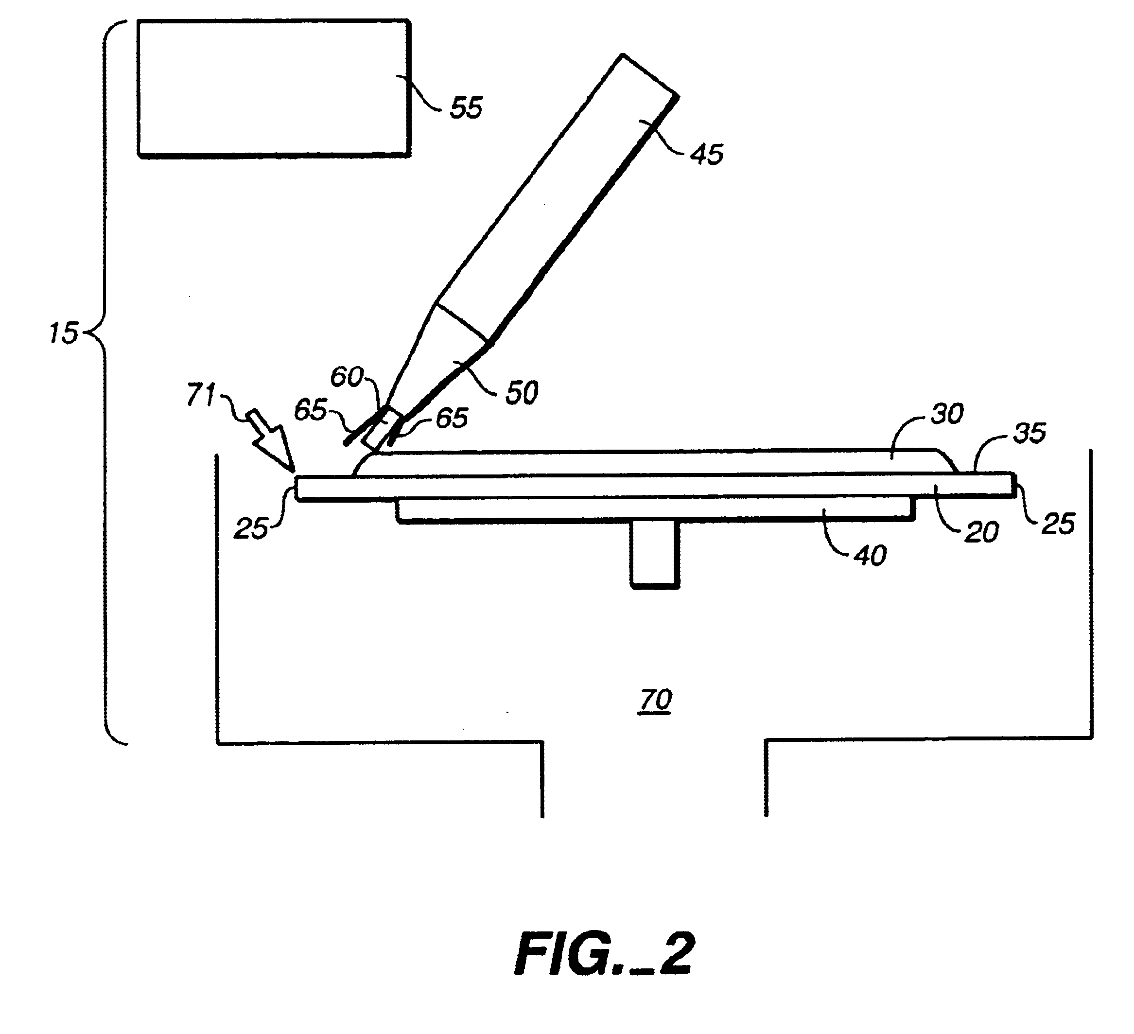
The present invention provides a method 100 of performing an edge clean operation on a semiconductor wafer 20, which is illustrated in FIG. 1. The system 15 used for performing the method 100 is illustrated in FIG. 2.

As illustrated in FIG. 2, the system 15 used for performing the method 100 includes the wafer 20 having an edge 25. Film 30 is attached to a top surface 35 of the wafer 20. The system 15 further includes a chuck 40, a laser 45 having a nozzle 50, and a video monitoring system 55. The laser 45 is capable of emitting a laser beam 60 through the nozzle 50. An inert purge gas 65 is also emitted throug...


PUM

PropertyMeasurementUnit
oblique angleaaaaaaaaaa
speedaaaaaaaaaa
poweraaaaaaaaaa

Abstract

A method for performing the edge clean operation on a semiconductor wafer. A laser beam is used to accurately clean the edge of the wafer. The wafer is clamped concentrically to a chuck and rotated at a selectable speed, preferably in the range of 10 rpm to 1,000 rpm. A laser beam of variable power is directed onto toward the edge of the wafer at an oblique angle through a nozzle through which an inert purge gas is simultaneously passed. The laser beam removes unwanted deposits at the edge of the wafer and the gas is used to blow away the residue and prevent slag buildup on other parts of the wafer. The process is preferably carried out in an exhausted chamber.

Description

BACKGROUND OF THE INVENTIONThe present invention relates to a method of performing the edge clean operation on semiconductor wafers. More specifically, the present invention relates to a method of using a laser to perform the edge clean operation on semiconductor wafers.One of the major problems gaining attention in wafer processing today is the edge related defects. Edge related defects contribute to lower die yield and lost revenue. A typical type of edge defect is the peeling of edge films due to poor adhesion to underlying layers.Many processing schemes have been devised and implemented to reduce edge related defects. The majority of processing schemes involve costly photo masking and etching steps in an attempt to reduce or eliminate the defects. The wafer is coated with photo resist and run through an edge bead removal step. The wafer is then etched in a plasma etcher to remove the films on the edge of the wafer. The resist is then stripped off in both a dry and then wet proce...

Claims


Application Information

Patent Timeline
Patent Type & Authority Patents(United States)
IPC IPC(8): B08B7/00H01L21/00H01L21/02H01L21/304
CPCB08B7/0042H01L21/67051H01L21/02087H01L21/02021
Inventor REDER, STEVENBERMAN, MICHAELBARBER, RENNIE
Owner BELL SEMICON LLC
Why Eureka
Try Eureka