

Application of a supercritical CO2 system for curing low k dielectric materials
- Summary
- Abstract
- Description
- Claims
- Application Information
AI Technical Summary
Benefits of technology
Problems solved by technology
Method used
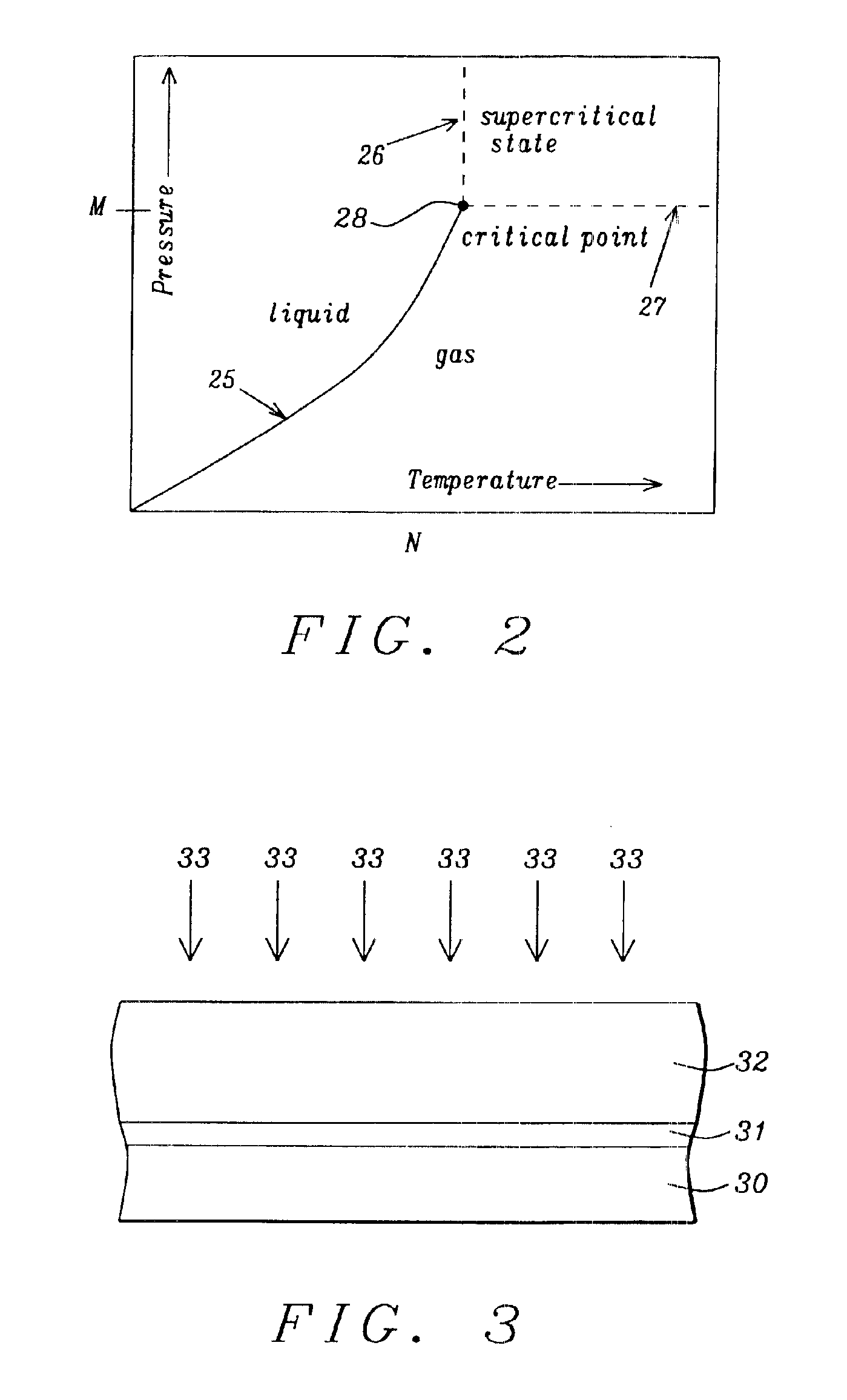
Image

Examples
first embodiment
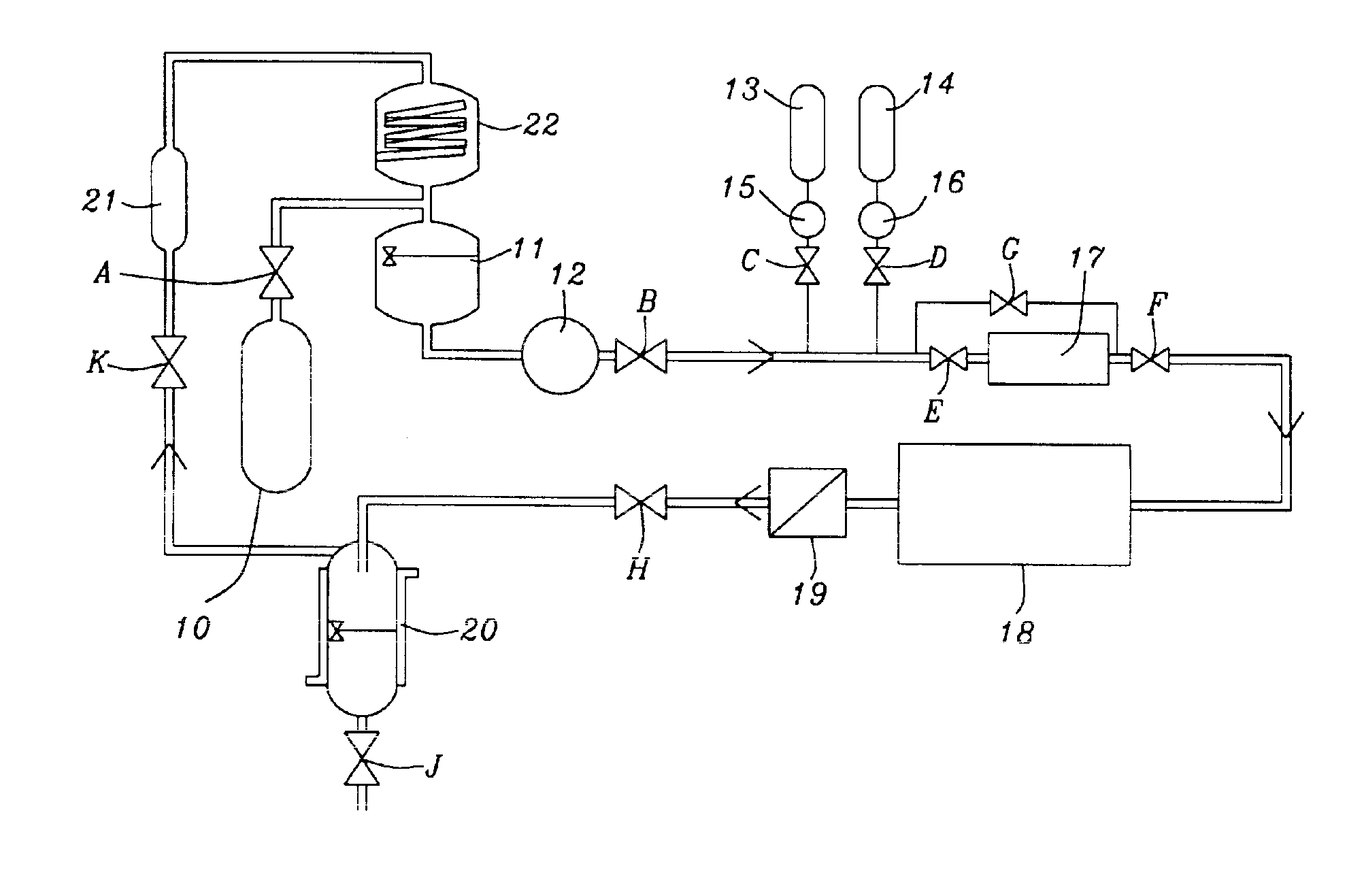
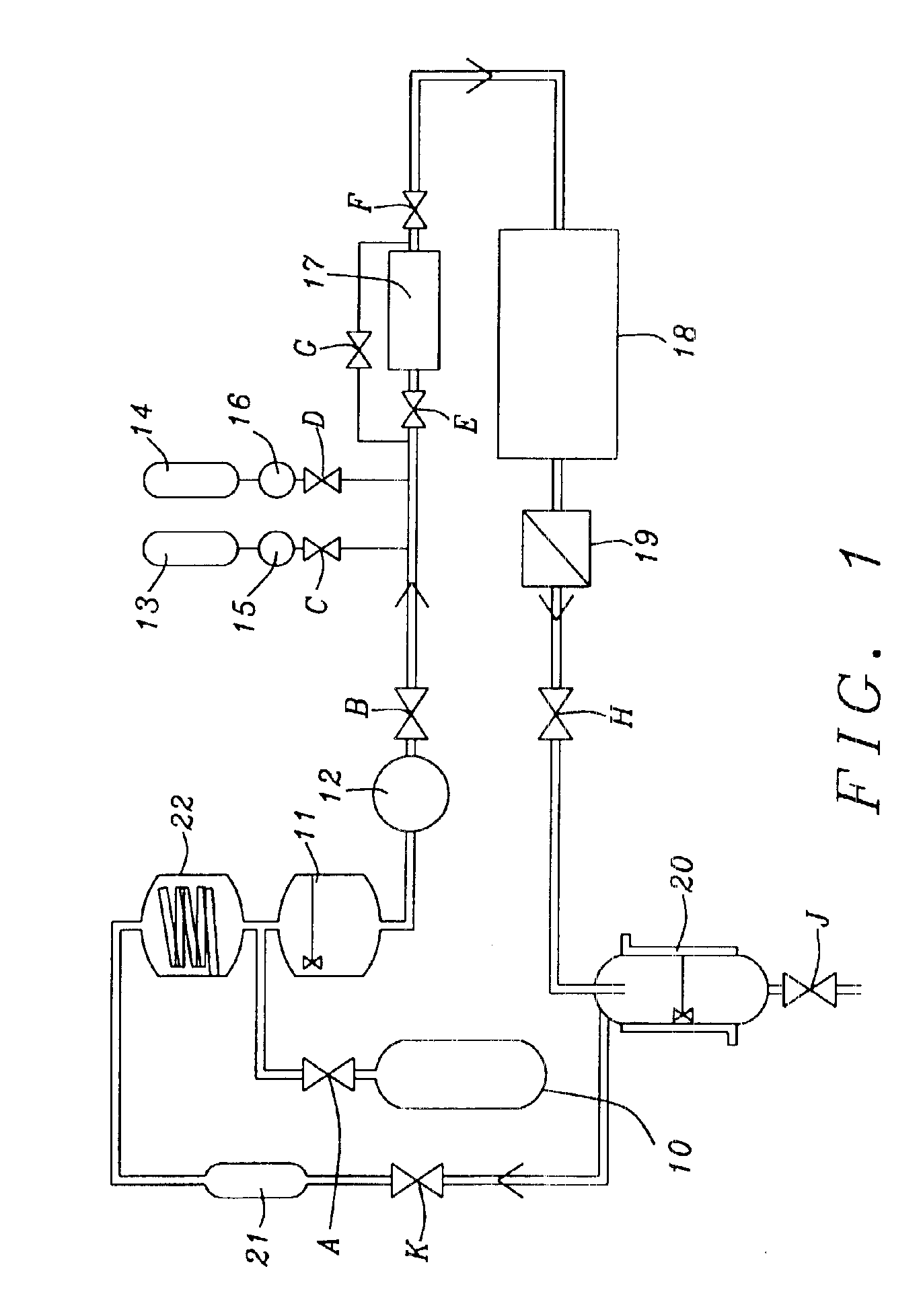
In one embodiment depicted in FIGS. 3-6, a low k dielectric layer that is treated by a method of this invention is part of an interconnect structure that is to be fabricated with a damascene method. In another embodiment, the low k dielectric layer to be cured may be in an interconnect structure that is fabricated by a process involving the deposition of a low k dielectric layer on a patterned metal layer. Those skilled in the art will recognize that the patterned metal layer may be comprised of a composite. For example, an anti-reflective layer such as TiN may be on a metal layer such as aluminum. Furthermore, there may be a conformal oxide liner on the composite metal layer. In this case, a spin-on low k dielectric material such as hydrogen silsesquioxane (HSQ) or methyl silsesquioxane (MSQ) is preferred for its ability to fill small gaps between the metal lines in the patterned metal layer. The advantages realized for treating a low k dielectric layer in a damascene scheme in the...
PUM
| Property | Measurement | Unit |
|---|---|---|
| Temperature | aaaaa | aaaaa |
| Temperature | aaaaa | aaaaa |
| Length | aaaaa | aaaaa |
Abstract
Description
Claims
Application Information