Substrate having repaired metallic pattern and method and device for repairing metallic pattern on substrate

Inactive Publication Date: 2005-04-05
HANGER SOLUTIONS LLC
View PDF24 Cites 4 Cited by
  • Summary
  • Abstract
  • Description
  • Claims
  • Application Information

AI Technical Summary

Benefits of technology

The present invention has been made to solve the above-mentioned problems. An object of the present invention is to provide a substrate having a repaired metallic pattern in which the defect is repaired while avoiding the generation of excessive heat and does not produce cracks in the repaired defective portion of the metal pattern. The invention also includes a method and a device for repairing a metallic pattern on a substrate for repairing an open defect of an electrode overlying a glass substrate of a liquid crystal display device and a defect of an opaque film of a mask with a thin film having good electric characteristics, that is, low electric resistance and good quality.
In the case described above, it is preferable that the above-mentioned organic compound is gold-resinate-based paste for low temperature baking. If the defective portion of the substrate is repaired by a gold thin film using this paste, in accordance with the invention, the defective part can be made extremely conductive as compared with the defective portions repaired by a conventional repairing material, such as conductive resin. Therefore, the defective portion does not produce heat and hence can prevent the glass substrate from suffering damage by heat.
A metallic thin film of metal deposited from the metallic organic compound is formed as a dense metallic layer by the above-mentioned techniques according to the present invention. Although the metallic thin film is very thin, it can have stable electric characteristics. Further, since the paste is preferably black and a semiconductor laser is used to heat the paste, only the paste formed in the defective portion absorbs laser light and is heated while other portions of the substrate do not absorb the laser light and are not heated. Therefore, non-defective portions of the glass substrate do not suffer damage from the heat generated by the laser.
The metallic pattern can be used as a mask of an opaque film by the above-mentioned removing process, and the metallic thin film deposited after heating and removing any protruding portions that can be used to form a mask having a metallic pattern of high quality.
When the above-mentioned repairing device is applied to the opaque film, any portions protruding from the metallic pattern need to be removed after the metallic pattern is repaired, and if the part is not removed, the metallic pattern will be of poor quality. Therefore, since any protruding portions of the metallic pattern are cut by a laser, such as YAG laser, to prevent the deterioration of quality, even if the metallic pattern is an expensive mask made of chromium on the glass substrate, it does not need to be scrapped, which can reduce costs.

Problems solved by technology

Also, the oxidation is detrimental to the electric characteristics and the oxidation process produce a large amount of heat.
In the method disclosed in (X), the conductive glass used for repairing the open defect in the electrode produces large resistance, and the process generates a large amount of heat when repairing the defect.
Similarly, the method disclosed in (Y) has structural problems in that resin containing conductive fine particles produces a large resistance and a large amount heat is needed in the process used to form the joined part.
In the method disclosed in (Z), a device referred to as a YAG laser for heating the conductive material is large in size and troublesome to handle.
Also, because the output of the device cannot be freely controlled, the conductive material is rapidly baked and cooled, which can produce cracks in the repaired part.
Further, since a line of a transparent electrode formed on the substrate of the liquid crystal display device is very small in width and in thickness, when the above-mentioned organ indium compound, the conductive glass or the adhesive containing conductive fine particles are used, it is difficult to make the joined part very thin.
Even if the joined part can be made thin, the quality of the joined part is not ensured because cracks are produced in the joined part.
In this regard, if the above-mentioned mask has a defect, the pattern formed on the transparent electrode also has a defect.
Also, opaque film of the above-mentioned mask sometimes has a defect and when the defect is repaired, the above-mentioned problems are also produced.
Still further, if the lithographic mask has a defect, the pattern is so fine that it is hard to repair the defect and hence the mask is scrapped.

Method used


Image

  • Substrate having repaired metallic pattern and method and device for repairing metallic pattern on substrate
  • Substrate having repaired metallic pattern and method and device for repairing metallic pattern on substrate
  • Substrate having repaired metallic pattern and method and device for repairing metallic pattern on substrate

Examples


Embodiment Construction

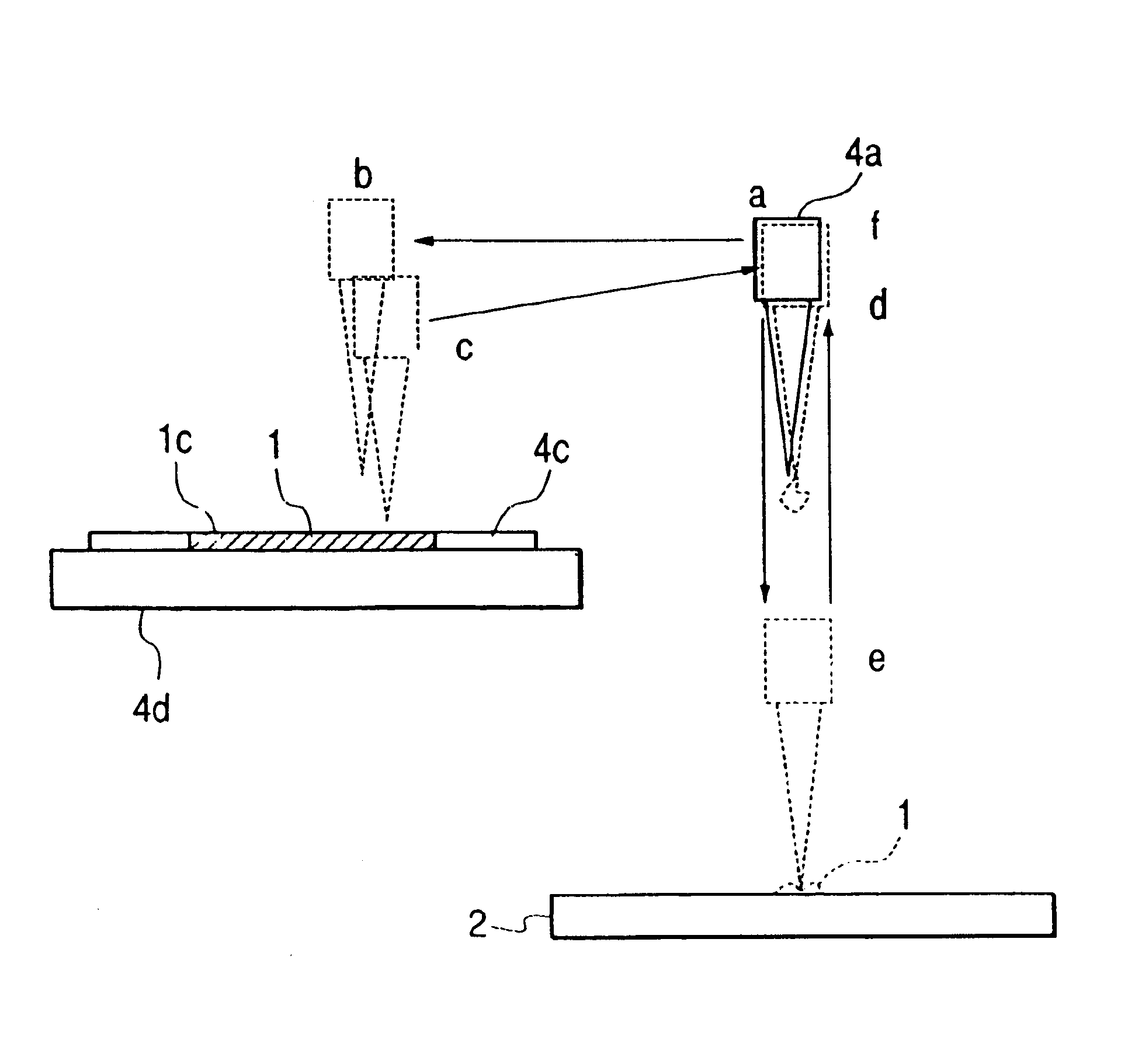
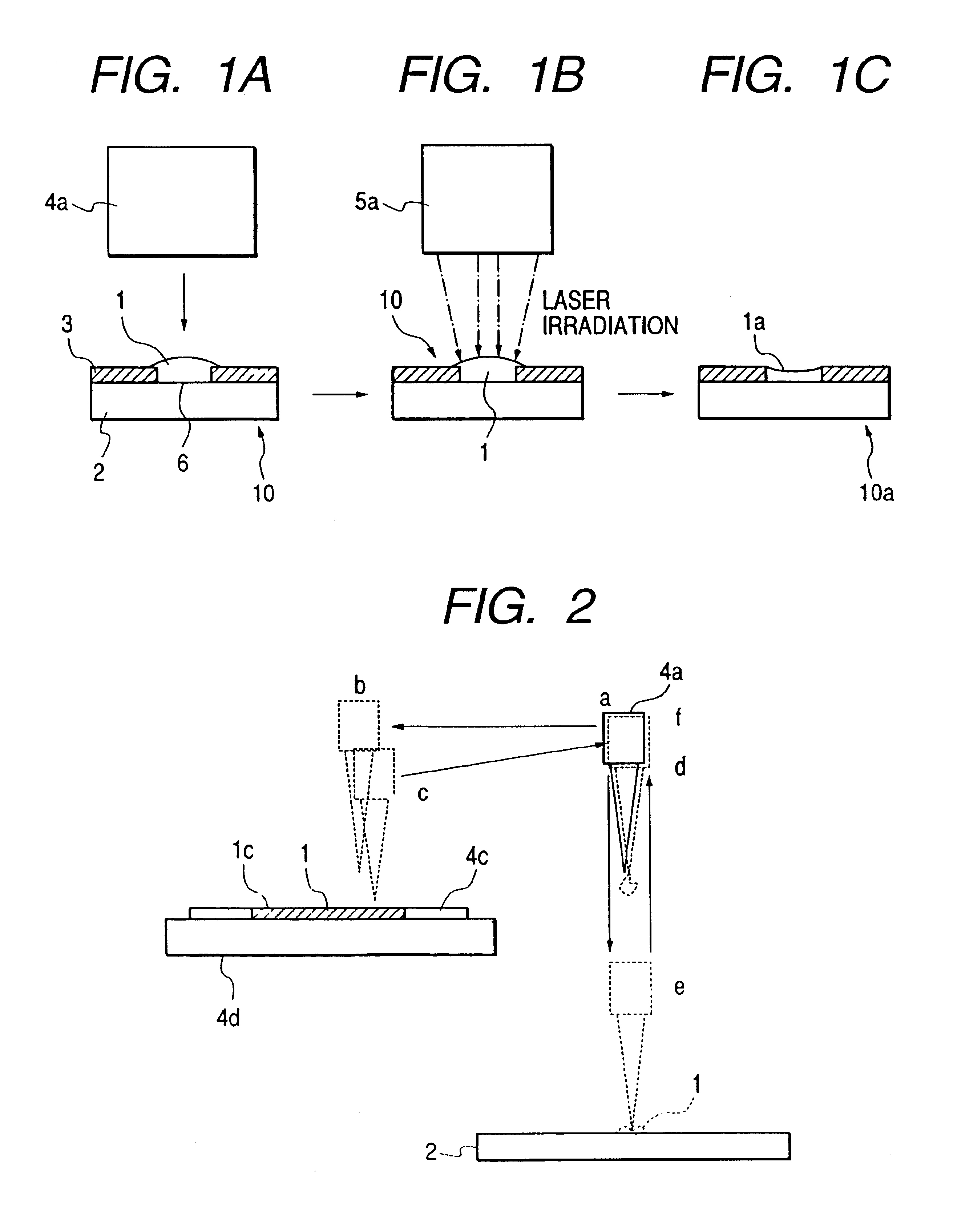
A substrate having an electrode repaired according to the present invention will be described with reference to the drawings.

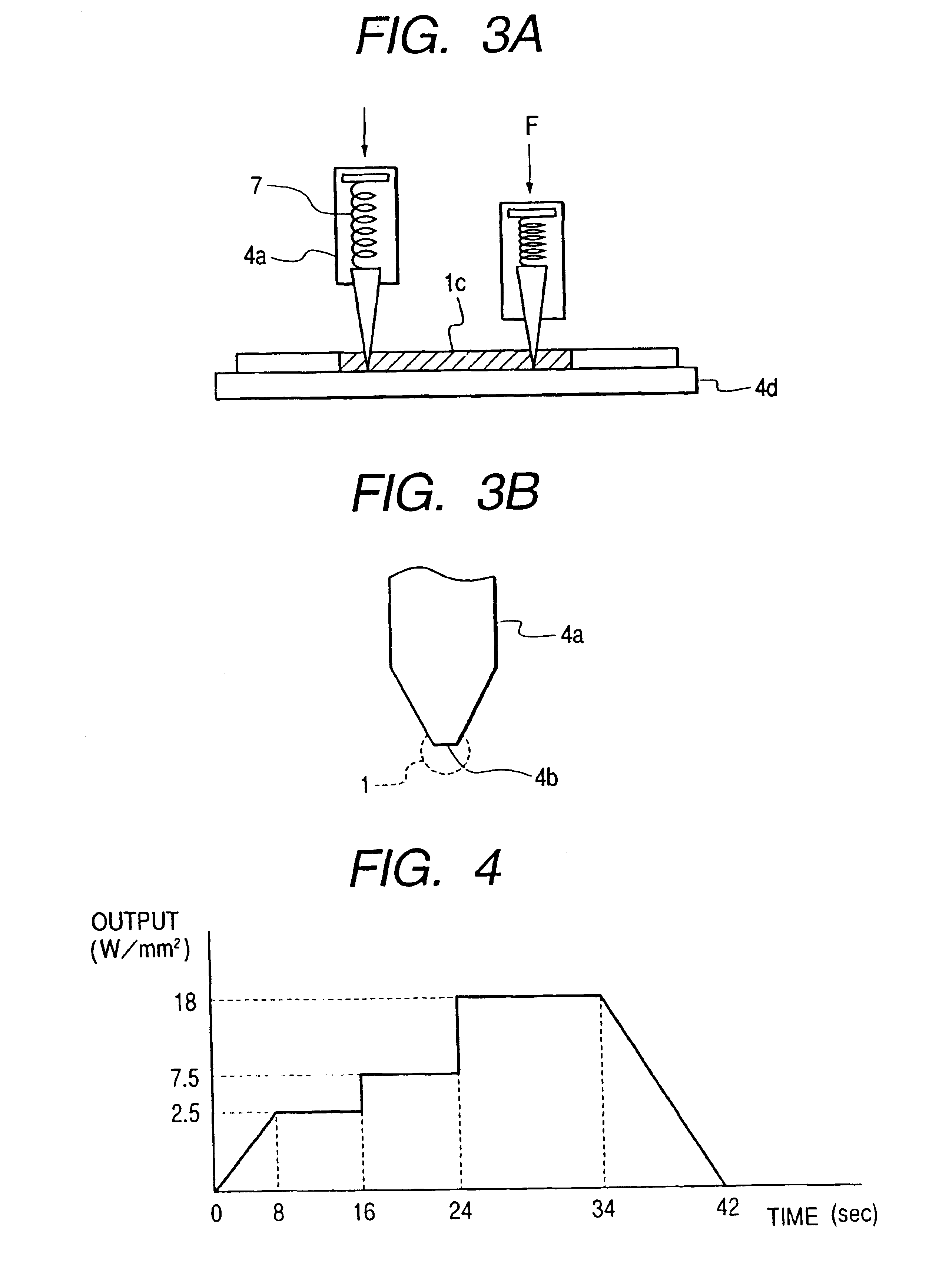
FIG. 1A, FIG. 1B and FIG. 1C schematically show steps of a method for repairing a broken defect, FIG. 1A shows a state in which paste 1 comprising metallic organic compound is applied on an open defect 6, FIG. 1B shows a state of heating the paste 1, and FIG. 1C shows the repaired state of the open defect 6 after heating.

In FIG. 1A, a substrate 10 shows a state of the substrate before repairing, in which paste 1 comprising metallic organic compound and an electrode 3 are laminated on a glass substrate 2. Glass substrate 2 is an ordinary substrate, and electrode 3 is made of ordinary material of ITO, or the like, and is formed in a line by patterning and etching on glass substrate 2 in an equal width and in an equal pitch. Further, paste 1 comprising metallic organic compound is formed by a transfer unit 4 on an open defect 6 of electrode 3 on the glass substra...


PUM

PropertyMeasurementUnit
Timeaaaaaaaaaa
Timeaaaaaaaaaa
Timeaaaaaaaaaa

Abstract

Paste comprising metallic organic compound, in particular, gold-based metallic organic compound is used as a conductive material for repairing open defects in a metal pattern. After applying the paste, the paste is baked to deposit a metal film. This can produce a very thin metallic film having low electric resistance. Further, a semiconductor laser is used as a heating unit to heat only the paste applied to the open defect. A heating profile having a multi-step baking process includes a provisional baking and main baking process followed by a cooling process to produce a high-quality thin metallic film having no cracks and a dense texture.

Description

BACKGROUND OF THE INVENTION1. Field of the InventionThe present invention relates to a substrate, such as a glass substrate, used for a liquid crystal display device and having a repaired defect in a metallic pattern or a mask of a semiconductor formed on the substrate and, and a method and a device for repairing the metallic pattern or the mask of the semiconductor on the substrate.2. Description of Related ArtIn recent years, a matrix type display device using a liquid crystal has been used widely as a display device for a computer instead of a display device using a cathode ray tube. Further, to increase the data displayed on a screen at one time, a liquid crystal display device or a plasma display device having a large screen or high definition has been developed. This has reduced yield and has increased defective substrates, and hence, the defective substrates are repaired to reduce costs of liquid crystal display device.An ordinary matrix type liquid crystal substrate is forme...

Claims


Application Information

Patent Timeline
IPC IPC(8): B23K26/34B23K26/00C23C20/00C23C20/04G03F1/00H05K3/22B05D3/06B05D5/00G02F1/13G02F1/1362C23C18/08C23C18/14C23C26/00G02F1/1343G03F1/72G09F9/30
CPCB23K26/34C23C18/08C23C18/14G03F1/72H05K3/225B23K26/3266B23K26/3293B23K35/0255B23K35/0261C03C17/00B23K35/025B05D3/06Y10T428/24917G02F2001/136263Y10S428/901B23K2201/40Y10T428/24926B05D5/005B23K26/32B23K2101/34B23K2101/40B23K2103/08B23K2103/50C03C17/23C03C2217/231C03C2217/255C03C2218/32C03C2218/34C23C18/143G02F1/136263B23K26/322G02F1/136259
Inventor SAKAI, OSAMUTAKAGI, KEIJI
Owner HANGER SOLUTIONS LLC
Why Eureka
Try Eureka