Organic electroluminescent display device

a display device and electroluminescent technology, applied in the direction of organic semiconductor devices, discharge tubes/lamp details, discharge tubes luminescnet screens, etc., can solve the problems of easy oxidation of devices, restricted single-crystal semiconductor substrates, and easy deterioration, and achieve high reliability

Inactive Publication Date: 2005-04-05
SEMICON ENERGY LAB CO LTD
View PDF28 Cites 42 Cited by
  • Summary
  • Abstract
  • Description
  • Claims
  • Application Information

AI Technical Summary

Benefits of technology

The object of the present invention is to overcome the problem as stated above, and to provide an organic EL display device of high reliability.

Problems solved by technology

On the other hand, however, it has been considered the disadvantage of the technology that the display device is restricted to one of reflection type, or spontaneous luminescence type because the substrate is opaque to visible light, or that the single-crystal semiconductor substrate is restricted to sizes available on the market.
However, an organic EL layer which serves as the basic portion of the organic El display device is very liable to oxidize, and it easily deteriorates in the presence of a slight amount of oxygen.
Besides, it has a low resistance to heat, and this also is a factor promoting oxidation.
The liability to oxidize is the cause of a short lifetime of the organic EL element, and has formed a serious obstacle in putting this element into practical use.

Method used


Image

  • Organic electroluminescent display device
  • Organic electroluminescent display device
  • Organic electroluminescent display device

Examples


Embodiment Construction

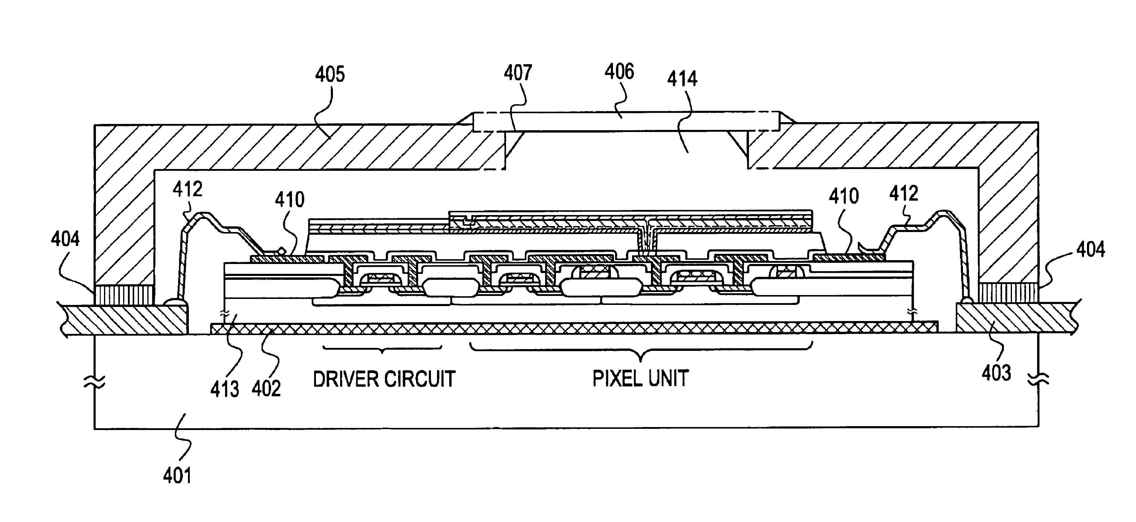
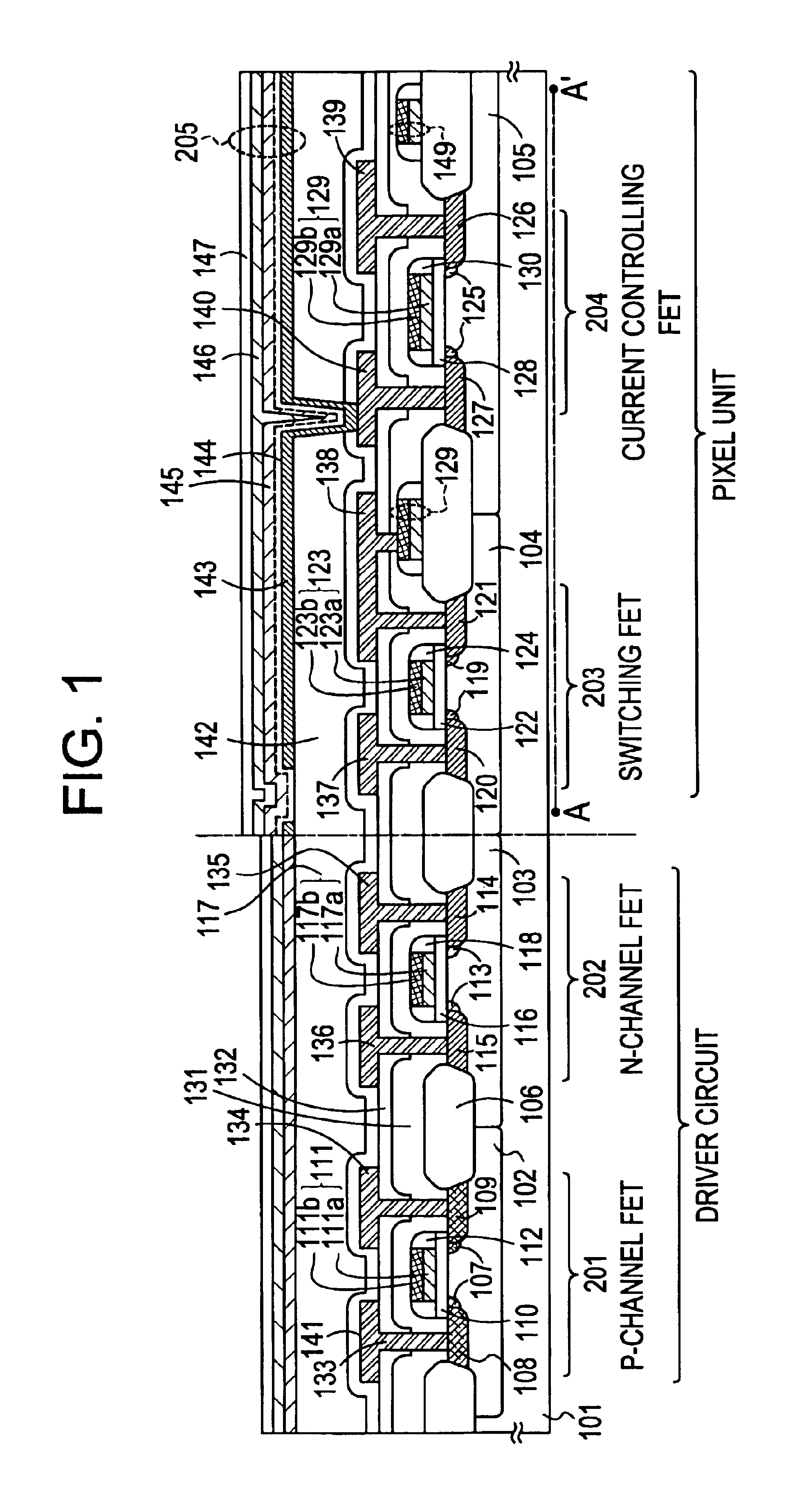
First, an organic EL display device according to the present invention will be described with reference to FIG. 1. The organic EL display device according to the present invention has such a structure that a pixel unit and driver circuits around the pixel unit are disposed using field effect transistors (FETs) of insulated gate type which are formed on a single-crystal semiconductor substrate (for example, single-crystal silicon substrate).

A substrate 101 is made of single-crystal silicon having a comparatively high resistance(for example, one of n-type at about 10[Ωcm]), and a p-well 102 and n-wells 103˜105 are formed in self-alignment therein. Adjacent FETs are isolated by a field oxide film 106. In forming the field oxide film 106, channel stoppers may be formed by introducing boron (B) into the selected parts of the substrate 101 in accordance with ion implantation.

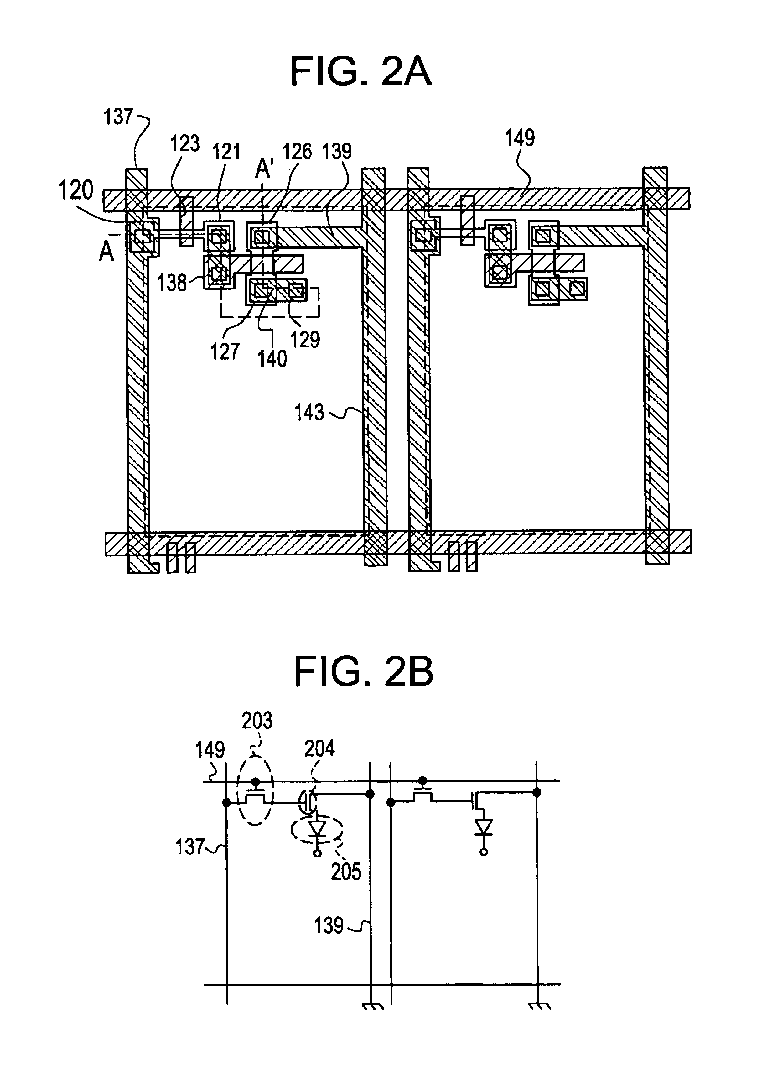
Gate insulating films 110, 116, 122 and 128 are formed by thermal oxidation. Gates 111, 117, 123 and 129 consist of...


PUM


Abstract

An organic EL display device of active matrix type wherein insulated-gate field effect transistors formed on a single-crystal semiconductor substrate are overlaid with an organic EL layer; characterized in that the single-crystal semiconductor substrate (413 in FIG. 4) is held in a vacant space (414) which is defined by a bed plate (401) and a cover plate (405) formed of an insulating material, and a packing material (404) for bonding the bed and cover plates; and that the vacant space (414) is filled with an inert gas and a drying agent, whereby the organic EL layer is prevented from oxidizing.

Description

BACKGROUND OP THE INVENTION1. Field of the InventionThe present invention relates to a semiconductor device having a circuit based on insulated-gate field effect transistors in which a single-crystal semiconductor is used for an active layer, and a method of fabricating the semiconductor device. More particularly, the present invention is well suited for applications to an electrooptic device which is typified by an organic electroluminescent display device wherein the same substrate is overlaid with a pixel unit and driver circuits disposed around the pixel unit, and to an electronic apparatus in which the electrooptic device is installed. Incidentally, here in this specification, the expression “semiconductor device” is intended to signify general devices which function by utilizing semiconductor properties, and it shall cover within its category the electrooptic device and the electronic equipment including this electrooptic device.2. Description of the Related ArtIn the field of...

Claims


Application Information

Patent Timeline
Patent Type & Authority Patents(United States)
IPC IPC(8): H01L27/32H01L51/52H01L27/28H01L51/50H05B33/04H05B33/00
CPCH01L27/3244H01L51/524H01L51/5259H01L51/5237H05B33/04H01L51/5275H01L51/5281H01L2251/5315H10K59/12H10K50/841H10K50/846H10K50/858H10K50/86H10K2102/3026H05B33/00H10K50/84
Inventor YAMAZAKI, SHUNPEIARAI, YASUYUKI
Owner SEMICON ENERGY LAB CO LTD
Why Eureka
Try Eureka