

Integrated digital circuit
- Summary
- Abstract
- Description
- Claims
- Application Information
AI Technical Summary
Benefits of technology
Problems solved by technology
Method used
Image

Examples
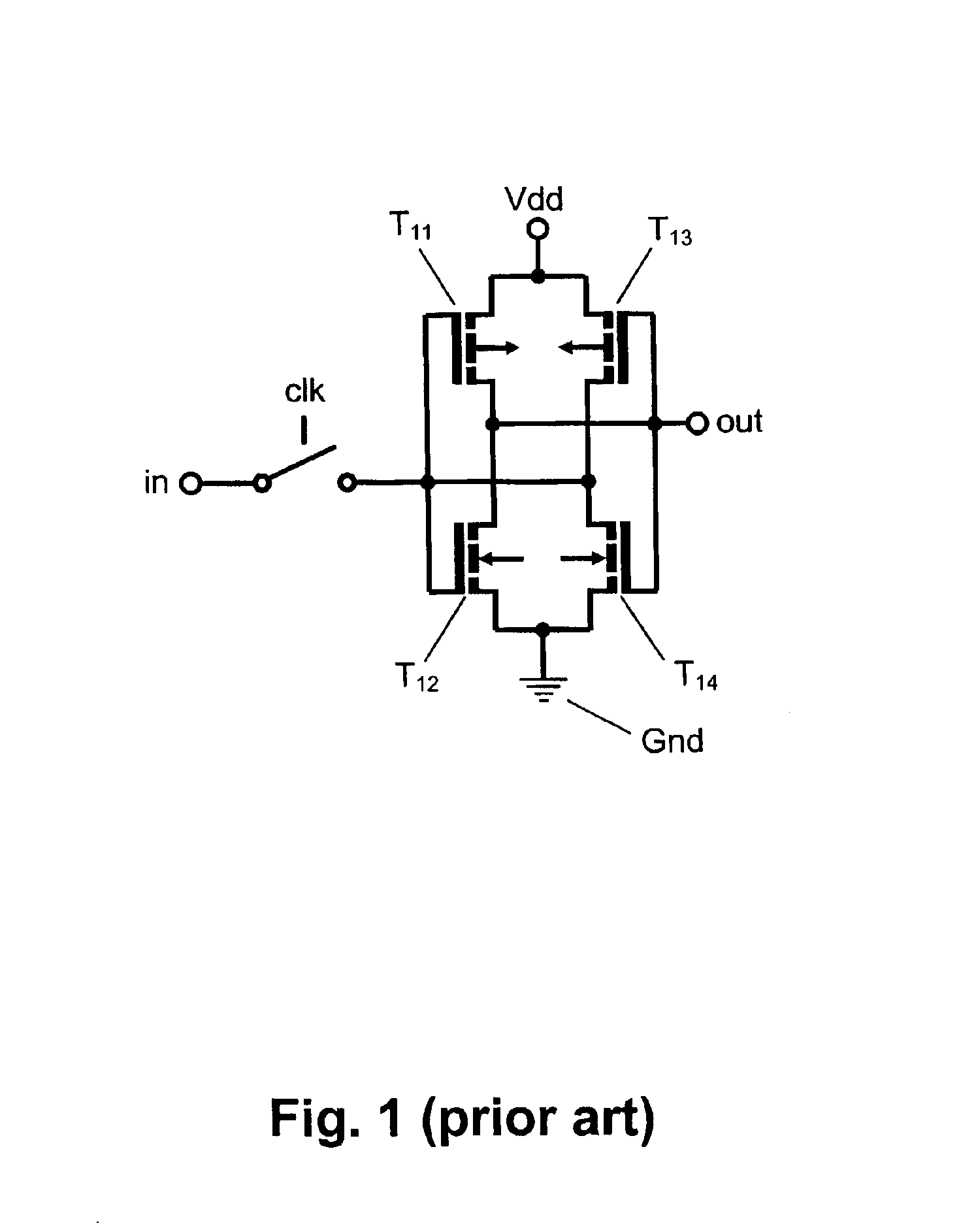
first embodiment
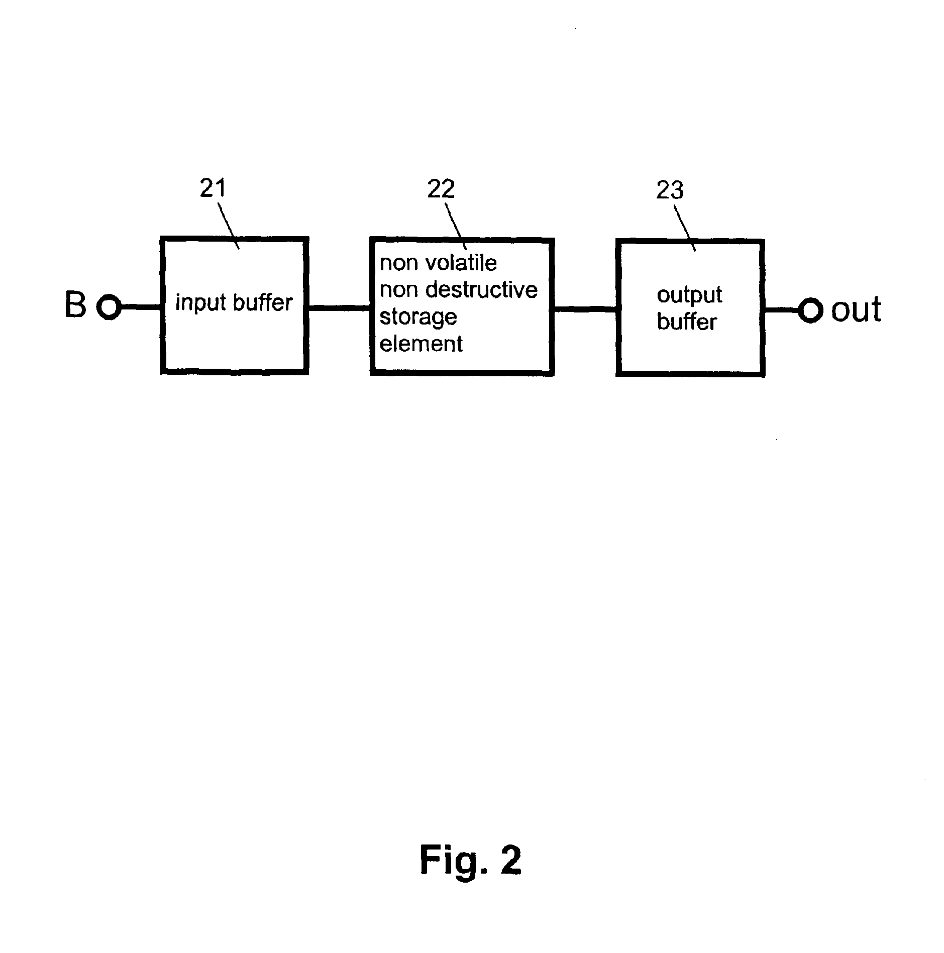
FIG. 2 is a block diagram which illustrates a part of the integrated digital circuit according to the invention in a general manner.
The circuit of FIG. 2 comprises an input buffer 21. The input of the input buffer 21 constitutes at the same time the input of the presented circuit. The output of the input buffer 21 is connected to the input of a non-volatile storage element 22, which can be programmed in a non-destructive manner. The output of the non-volatile storage element 22 is connected to an input of an output buffer 23. The output of the output buffer 23 constitutes at the same time the output of the presented circuit. The input buffer 21 and the output buffer 23 form a logic circuit portion which takes one of at least two different logic states in accordance with provided control signals.
When an input signal ‘B’ is applied to the circuit of FIG. 2, the input buffer 21 buffers a state represented by the input signal ‘B’ as long as power is supplied to the input buffer 21 and a...
second embodiment
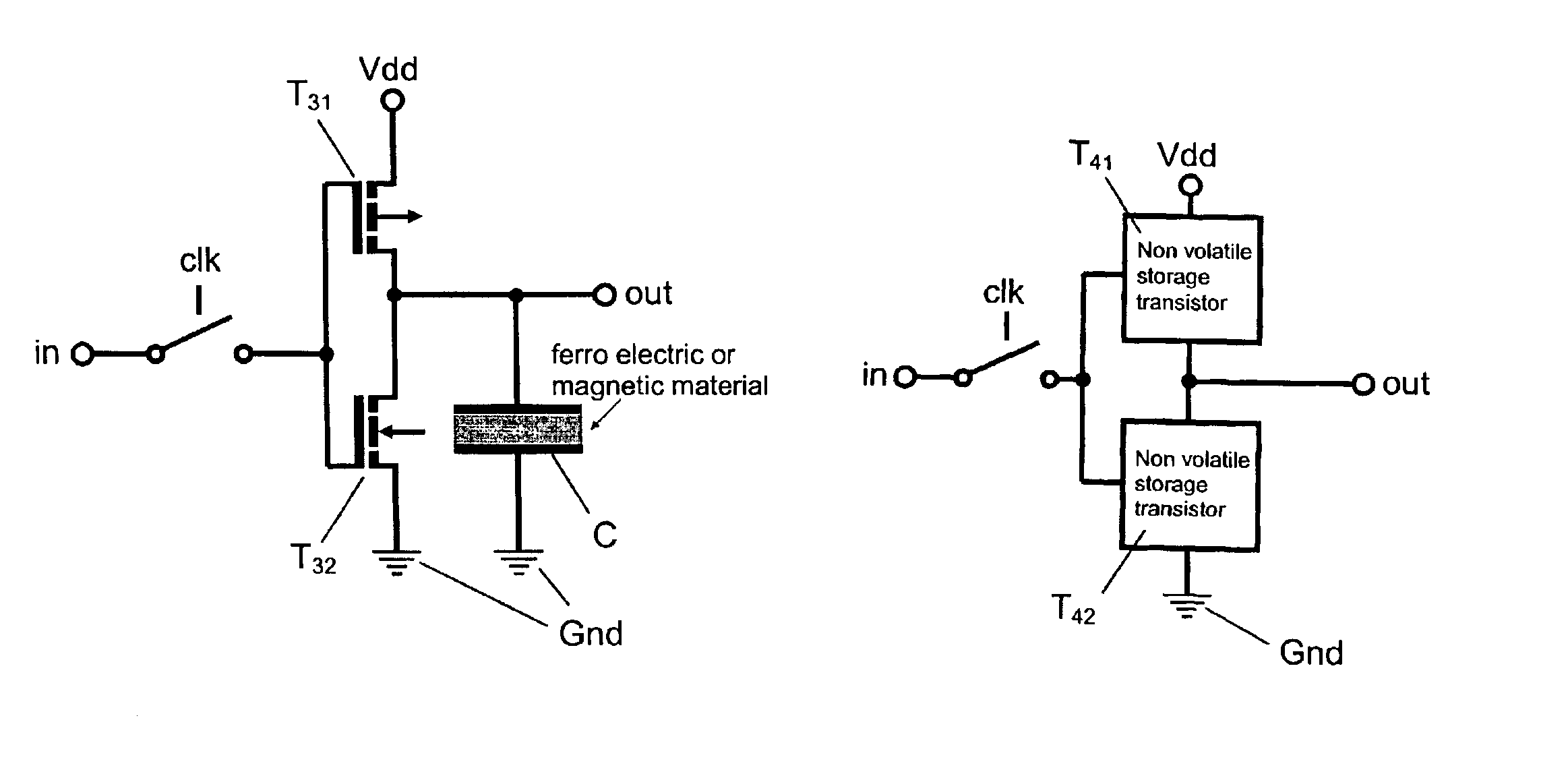
FIG. 4 illustrates another modified CMOS latch as part of an integrated digital circuit according to the invention.
Like the circuit of FIG. 3, the circuit of FIG. 4 comprises a pair of CMOS transistors T41, T42, which is arranged between a voltage supply Vdd and ground Gnd and which is connected to a clocked input “in” and to an output “out”. The clocking is represented again by a switch clk arranged between the input “in” and the gates of the transistors T41, T42. Also the basic functions of the pair of CMOS transistors T41, T42 for providing a high and a low output voltage at output “out” is the same as in the embodiment presented in FIG. 2. MOSFETs T41 and T42 thus constitute in this embodiment the logic circuit portion of the integrated digital circuit according to the invention.
In this second embodiment, however, a non-volatile storage component is integrated directly into the transistors T41, T42. This leads to bi-stable transistors T41, T42 which are usable as a storage eleme...
PUM
 Abstract
Description
Claims
Application Information