Organic vertical cavity lasing device having organic active region

Inactive Publication Date: 2005-04-05
EASTMAN KODAK CO
View PDF27 Cites 12 Cited by
  • Summary
  • Abstract
  • Description
  • Claims
  • Application Information

AI Technical Summary

Benefits of technology

It is an advantage of the present invention to improve the operation of a vertical cavity laser design incorporating high reflectance top and bottom dielectric stacks, having gain regions including either small-molecular weight organic material or

Problems solved by technology

Such high power densities can only be obtained by using other lasers as the pump sources, precluding that route for inorganic laser cavities.
This result is highly significant for amorphous organic laser syst

Method used


Image

  • Organic vertical cavity lasing device having organic active region
  • Organic vertical cavity lasing device having organic active region
  • Organic vertical cavity lasing device having organic active region

Examples


example 1

Solution Ultaviolet (UV) absorption spectra and fluorescent emission spectra of materials demonstrate useful dopant and host materials. The solution UV absorption spectra and fluorescent emission spectra of representative materials are given in FIGS. 3-46. All solution spectra are from ethyl acetate solutions with the exception of L59 (THF), L60 (water) and L62 (sucrose octaacetate).

The Table indicates overlap of the emission of the host material with the absorbance of the dopant materials. An “X” indicates at least 5% host emission relative to local emission maximum at a wavelength that has at least 5% dopant absorbance relative to local absorbance maximum. A “0” indicates no (or less) overlap.

TABLEHosts:F2CO1DPPAD1D4D2Dopants:XXXXXXL56XXXXXXL2XXXXXXL5XX00XXL60XXXXXXL1XXXXXXL50X0XXXXL52XXXXXXL58X0XXXXL39XXXXXXL30XXXXXXL57XXXXXXL47XXXXXXL59XXXXXXL61XXXXXXL62XXXXXXF2na0XXXX

Clearly there are numerous combinations of host and dopant materials where the emission of the host material ove...

example 2

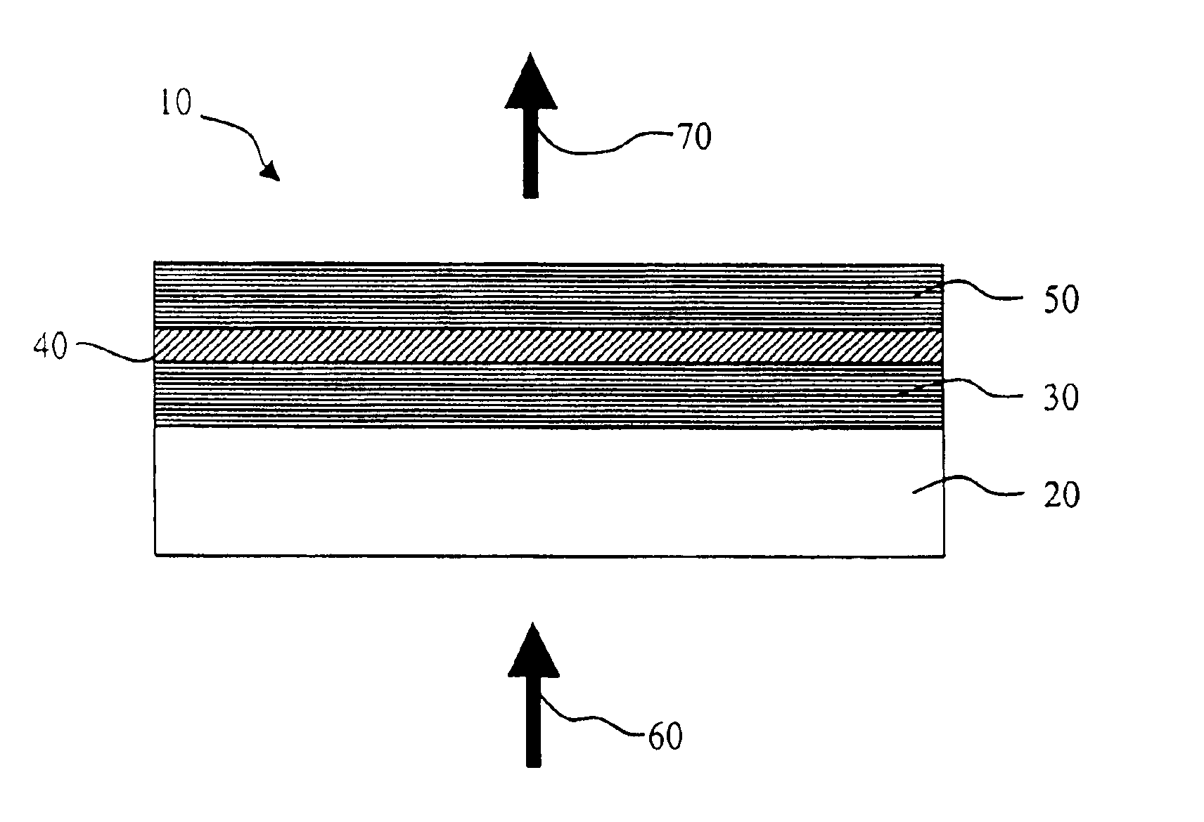
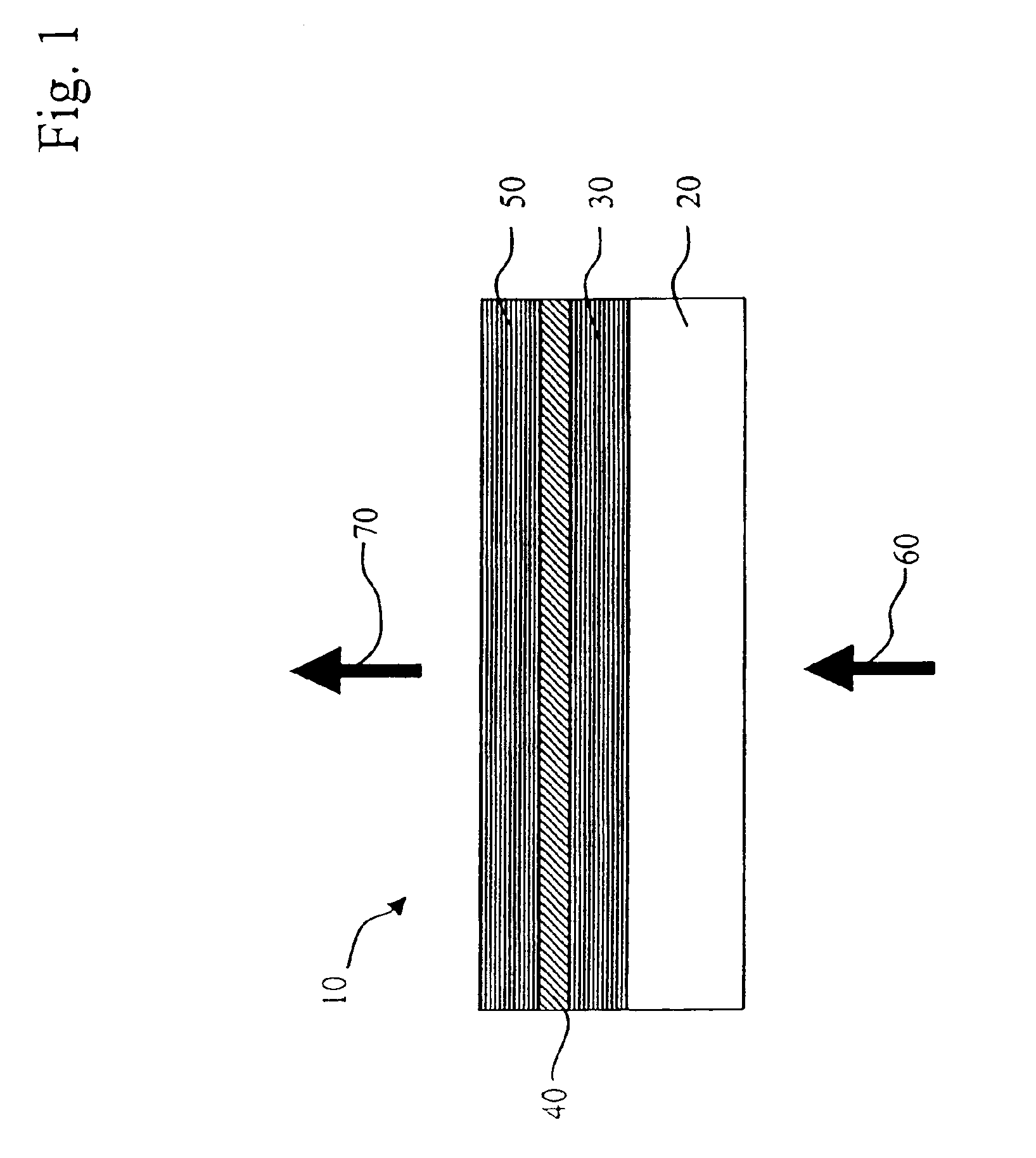
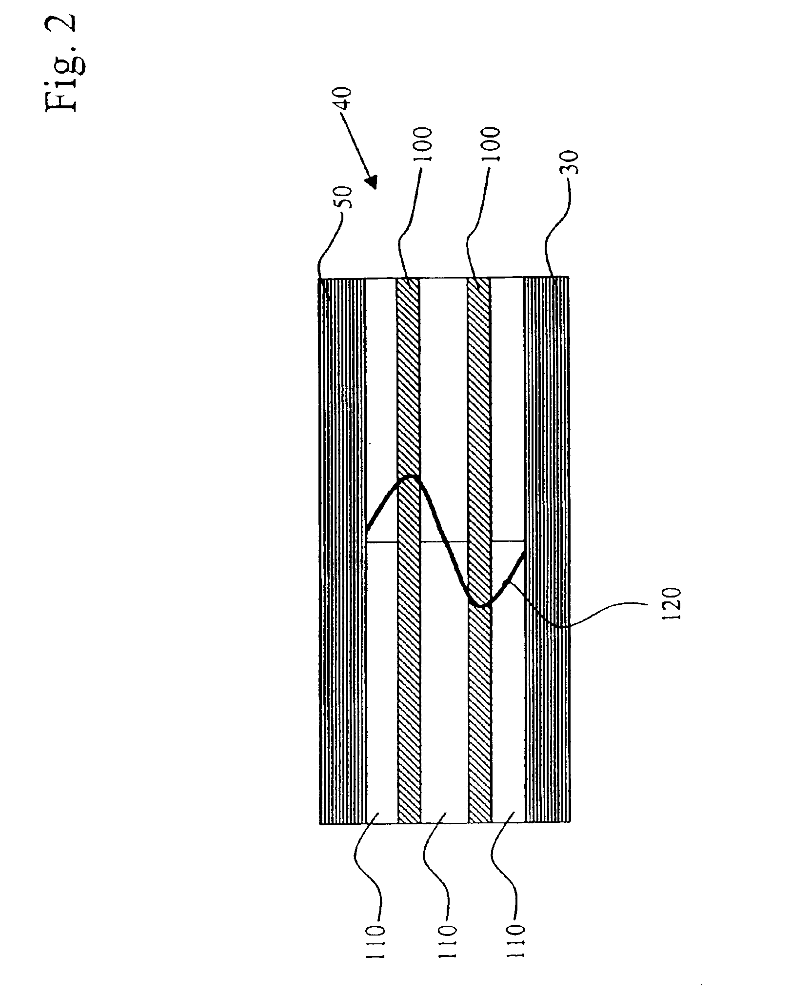
To test the devices for both their spectral and power characteristics, an organic vertical cavity laser structure 10 was deposited on a 4-inch silicon substrate. Over the substrate was deposited, by conventional electron beam deposition, the bottom dielectric stack 30, which was composed of alternating low and high refractive index layers of SiO2 and TiO2, respectively. The bottom dielectric stack had a peak reflectance of ˜99.95% at 660 nm. On top of the bottom dielectric stack was deposited, by high-vacuum thermal evaporation, the active region 40. The composition of the active region was 190 nm of TAPC, 20 nm of Alq plus a dopant, and 188 nm of TAPC. In one example, the dopant was L39 at a concentration of 1%; while, for the other case the dopant was L62 at a concentration of 0.5%. Following the active region 40 was deposited the top dielectric stack 50 composed of alternating layers of SiO2 and TiO2, such that its resulting measured peak reflectance was 99.85% at 660 nm. The top...

example 3

In this example, a comparison was made for laser devices containing green dopants. The device structure was analogous to that of Example 2, except the thicknesses of the active region layers were 137 nm of TAPC, 50 nm of Alq plus a dopant, and 122 nm of TAPC. The four dopants for this example are 0.5% of L30, 0.75% of L55, 0.75% of L54, and 0.75% of L53. The bottom dielectric stack 30 had a peak reflectance of ˜99.98% at 560 nm, while the top dielectric stack 50 had a peak reflectance of ˜99.3% at 560 nm. At a pump-beam power density on the device surface of ˜10 W / cm2, the measured spectral and intensity characteristics for the four cases are given in the table below.

EmissionActive RegionIntensityLinewidthwavelengthIntensitydopant(5 KHz)(5 KHz)(5 KHz)(5 MHz) 0.5% L3051861.3 nm562 nm51 × 1050.75% L5535221.2 nm567 nm30 × 1050.75% L5451001.4 nm557 nm41 × 1050.75% L5344001.1 nm562 nm37 × 105

As can be seen from the table, the device containing the L30 dopant produced the most intense las...


PUM

PropertyMeasurementUnit
Nanoscale particle sizeaaaaaaaaaa
Fractionaaaaaaaaaa

Abstract

An organic vertical cavity laser light producing device includes a bottom dielectric stack reflective to light over a predetermined range of wavelengths; an organic active region for producing laser light, and having an organic active region including emissive material; and a top dielectric stack spaced from the bottom dielectric stack and reflective to light over a predetermined range of wavelengths. Pump-beam light is transmitted and introduced into the organic active region through at least one of the dielectric stacks. The organic active region includes one or more periodic gain region(s) and organic spacer layers disposed on either side of the periodic gain region(s) and arranged so that the periodic gain region(s) is aligned with the antinodes of the device's standing wave electromagnetic field, and wherein the spacer layers are substantially transparent to the laser light.

Description

FIELD OF INVENTIONThis invention relates to the field of light-emitting devices. More specifically, this invention relates to organic-based solid-state lasers.BACKGROUND OF THE INVENTIONVertical cavity surface emitting lasers (VCSELs) based on inorganic semiconductors (e.g., AlGaAs) have been developed since the mid-80's (K. Kinoshita et al., IEEE J. Quant. Electron. QE-23, 882, 1987). They have reached the point where AlGaAs-based VCSELs emitting at 850 nm are manufactured by a number of companies and have lifetimes beyond 100 years (K. D. Choquette et al., Proc. IEEE 85, 1730, 1997). With the success of these near-infrared lasers in recent years, attention has turned to other inorganic material systems to produce VCSELs emitting in the visible wavelength range (C. Wilmsen et al., Vertical-Cavity Surface-Emitting Lasers, Cambridge University Press, Cambridge, 2001). There are many fruitful applications for visible lasers, such as display, optical storage reading / writing, laser prin...

Claims


Application Information

Patent Timeline
IPC IPC(8): B23K11/31B23K11/25B23K11/30
CPCB23K11/255B23K11/315B23K11/31
Inventor KAHEN, KEITH B.VARGAS, J. RAMONKONDAKOV, DENIS Y.BROWN, CHRISTOPHER T.COSIMBESCU, LELIAJARIKOV, VIKTOR
Owner EASTMAN KODAK CO
Why Eureka
Try Eureka