Combined eddy current sensing and optical monitoring for chemical mechanical polishing

Inactive Publication Date: 2005-04-12
APPLIED MATERIALS INC
View PDF60 Cites 29 Cited by
  • Summary
  • Abstract
  • Description
  • Claims
  • Application Information

AI Technical Summary

Benefits of technology

Implementations of the invention can include zero or more of the following possible advantages. The endpoint detector can sense the polishing endpoint of a metal layer in-situ. The magnetic field apparatus for the endpoint detector can be embedded in the platen below a polishing pad. The magnetic field apparatus can be protected from polishing environment, e.g., corrosive slurry. The endpoint detector need not use complex electronics. Polishing can be stopped with reasonable accuracy. Overpolishing and underpolishing substrate can be reduced, thereby improving yield and throughput.

Problems solved by technology

One problem in CMP is determining whether the polishing process is complete, i.e., whether a substrate layer has been planarized to a desired flatness or thickness, or when a desired amount of material has been removed.
On the other hand, underpolishing (removing too little) of a conductive layer leads to electrical shorting.
This is a time-consuming procedure that reduces the throughput of the CMP apparatus.
Alternatively, the examination might reveal that an excessive amount of material has been removed, rendering the substrate unusable.
Unfortunately, the proposed eddy current sensing techniques typically require complex electronics.

Method used


Image

  • Combined eddy current sensing and optical monitoring for chemical mechanical polishing
  • Combined eddy current sensing and optical monitoring for chemical mechanical polishing
  • Combined eddy current sensing and optical monitoring for chemical mechanical polishing

Examples


Embodiment Construction

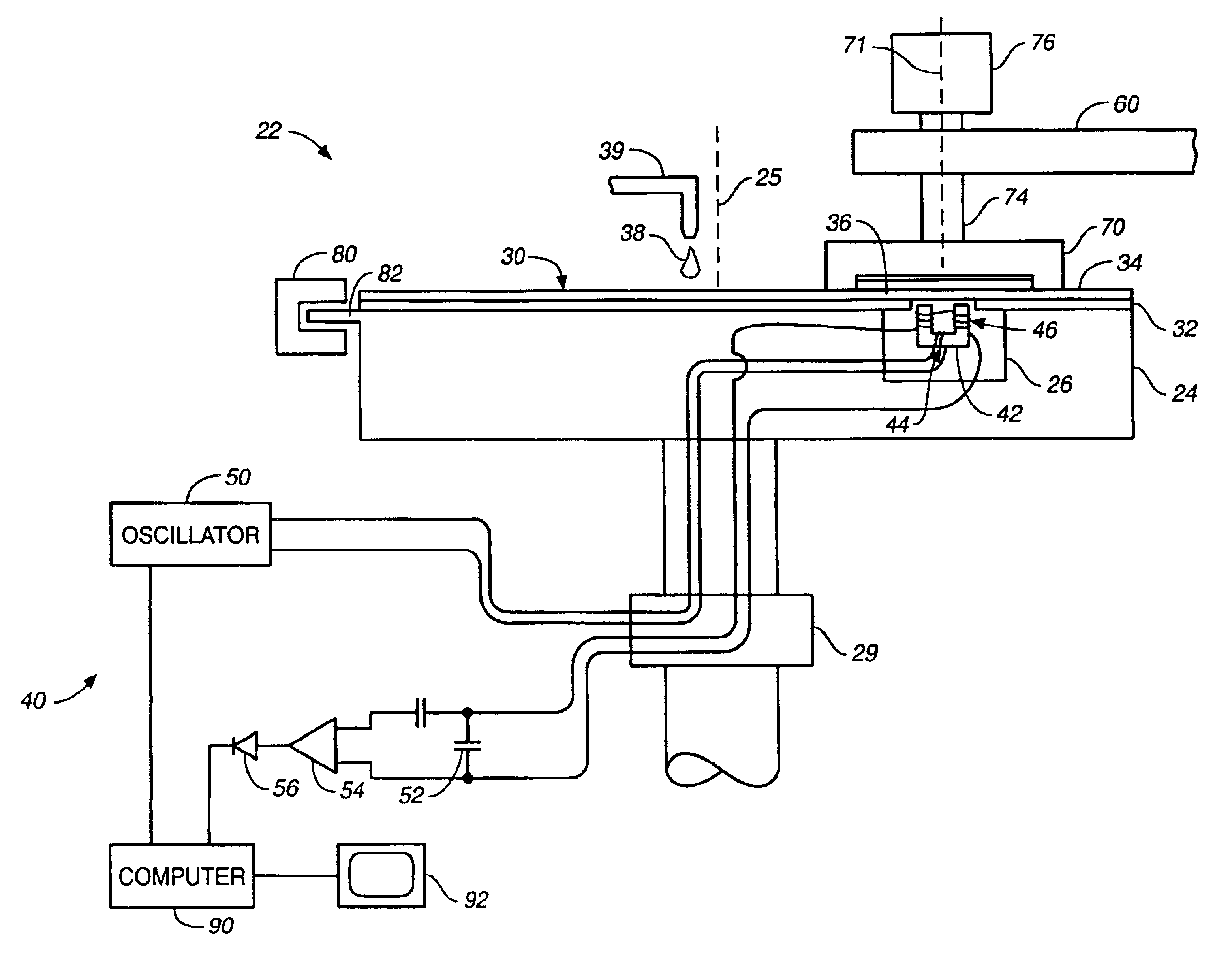
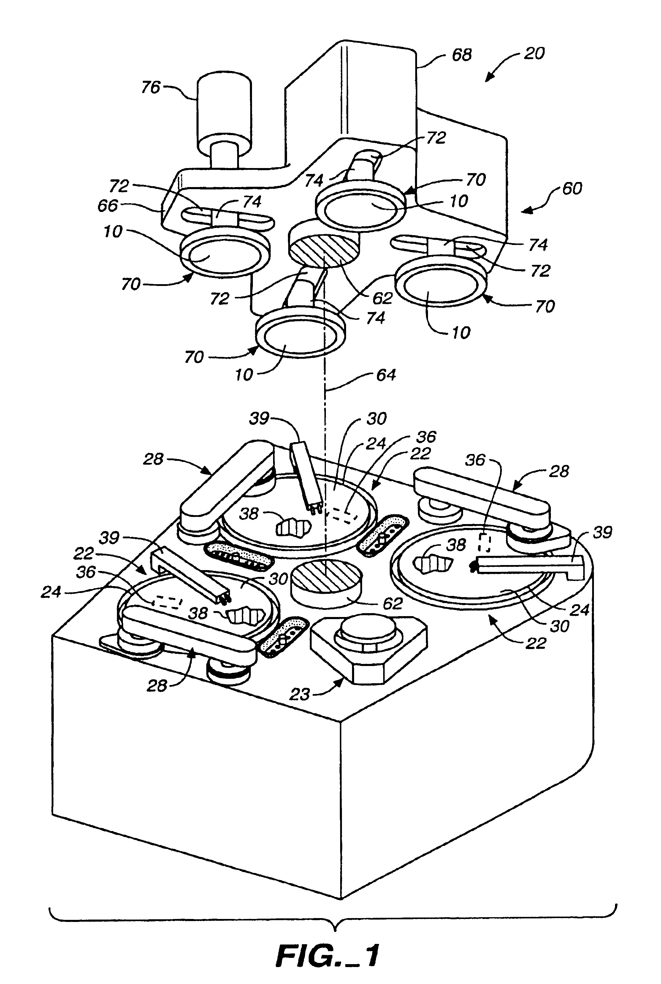
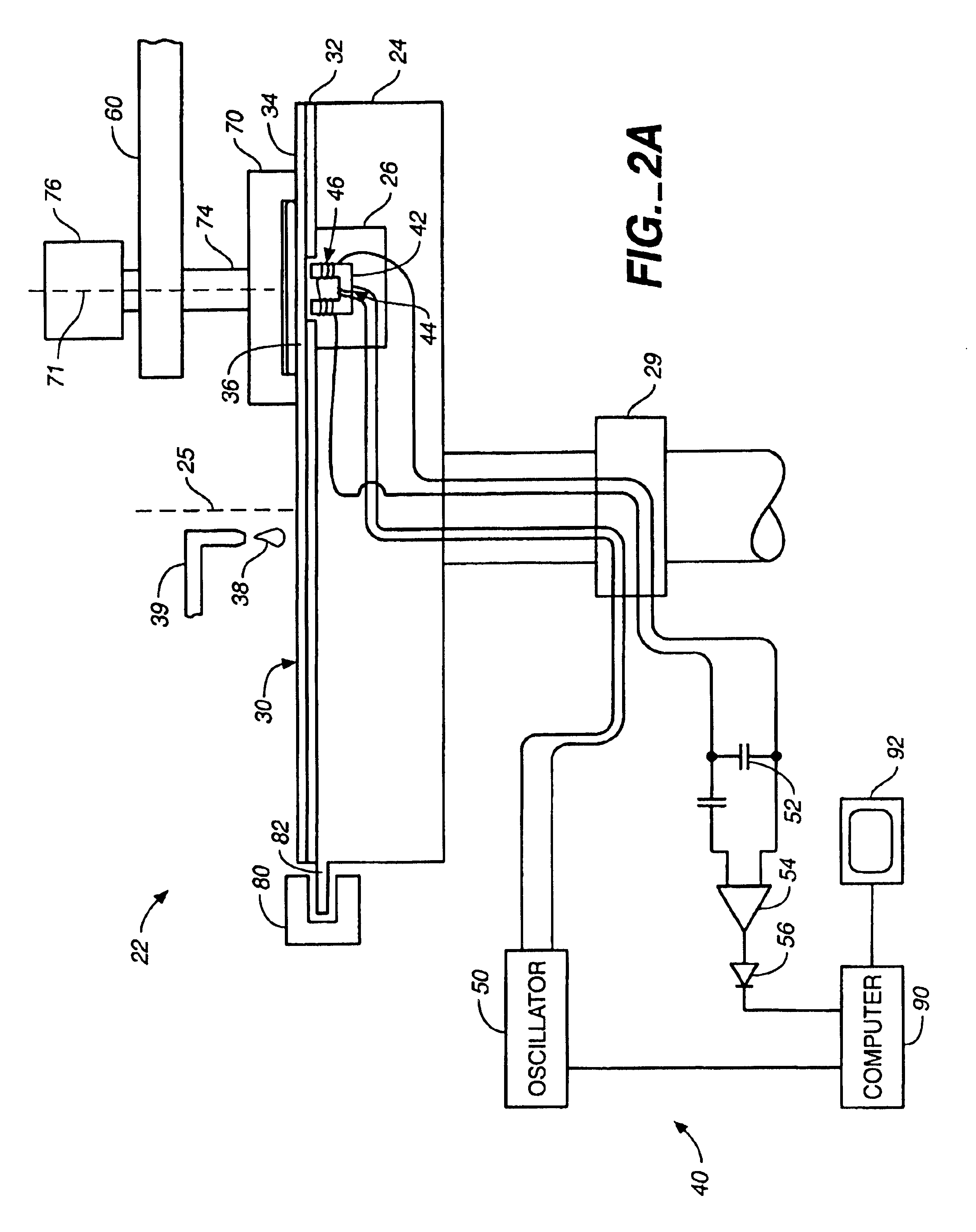
Referring to FIGS. 1 and 2A, one or more substrates 10 can be polished by a CMP apparatus 20. A description of a similar polishing apparatus 20 can be found in U.S. Pat. No. 5,738,574, the entire disclosure of which is incorporated herein by reference. Polishing apparatus 20 includes a series of polishing stations 22 and a transfer station 23. Transfer station 23 transfers the substrates between the carrier heads and a loading apparatus.

Each polishing station includes a rotatable platen 24 on which is placed a polishing pad 30. The first and second stations can include a two-layer polishing pad with a hard durable outer surface or a fixed-abrasive pad with embedded abrasive particles. The final polishing station can include a relatively soft pad. Each polishing station can also include a pad conditioner apparatus 28 to maintain the condition of the polishing pad so that it will effectively polish substrates.

A two-layer polishing pad 30 typically has a backing layer 32 which abuts th...


PUM


Abstract

A chemical mechanical polishing apparatus has a polishing pad, a carrier to hold a substrate against a first side of the polishing surface, and a motor coupled to at least one of the polishing pad and carrier head for generating relative motion therebetween. An eddy current monitoring system is positioned to generate an alternating magnetic field in proximity to the substrate, an optical monitoring system generates a light beam and detects reflections of the light beam from the substrate, and a controller receives signals from the eddy current monitoring system and the optical monitoring system.

Description

BACKGROUNDThe present invention relates generally to chemical mechanical polishing of substrates, and more particularly to methods and apparatus for monitoring a metal layer during chemical mechanical polishing.An integrated circuit is typically formed on a substrate by the sequential deposition of conductive, semiconductive or insulative layers on a silicon wafer. One fabrication step involves depositing a filler layer over a non-planar surface, and planarizing the filler layer until the non-planar surface is exposed. For example, a conductive filler layer can be deposited on a patterned insulative layer to fill the trenches or holes in the insulative layer. The filler layer is then polished until the raised pattern of the insulative layer is exposed. After planarization, the portions of the conductive layer remaining between the raised pattern of the insulative layer form vias, plugs and lines that provide conductive paths between thin film circuits on the substrate. In addition, ...

Claims


Application Information

Patent Timeline
IPC IPC(8): B24B37/04B24B49/02B24B49/04B24B49/12B24B49/10B24B1/00B24B37/013
CPCB24B37/013B24B49/02G01B7/105B24B49/10B24B49/12B24B49/04
Inventor JOHANSSON, NILSSWEDEK, BOGUSLAW A.BIRANG, MANOOCHER
Owner APPLIED MATERIALS INC
Why Eureka
Try Eureka