Supercharge Your Innovation With Domain-Expert AI Agents!

Structure of LCD manufactured by one-drop fill technology including a substrate with transparent conductive patterns

a liquid crystal display and one-drop fill technology, applied in the direction of optics, non-linear optics, instruments, etc., can solve the problems of large pollution of lcd panels, difficult and inability to meet the requirements of lcd injection

Inactive Publication Date: 2005-04-12
WUHAN CHINA STAR OPTOELECTRONICS TECH CO LTD
View PDF5 Cites 12 Cited by
  • Summary
  • Abstract
  • Description
  • Claims
  • Application Information

AI Technical Summary

Benefits of technology

It is an object of the present invention to provide a method and structure to reduce the pollution of liquid crystal in a liquid crystal display manufactured by one drop fill (ODF) technology.
It is another object of the present invention is to provide a method and structure to improve an ultraviolet-type seal pre-harden condition to decrease the pollution problem.
It is further another object of the present invention is to improve the pollution problem of the liquid crystal to increase the quality and the yield of the liquid crystal displays.
To accomplish the above objectives, the present invention provides a method for fabricating liquid crystal display with one drop fill technology. The method comprises the following steps. First, a first substrate with a conductive pattern layer formed by peripheral circuits is provided. The conductive pattern layer is made of an indium tin oxide material. Second, a second substrate with a black matrix layer to avoid light leakage of the liquid crystal display is provided. Then, an ultraviolet-type seal is spread on the first substrate. A liquid crystal material is dropped on the first substrate. The first substrate and the second substrate are glued together in a vacuum chamber. The seal is exposed to an ultraviolet ray from the first substrate to pre-harden the seal for a predetermined period. Finally, the seal is heated in a heating chamber.
In another aspect, the present invention provides a structure of liquid crystal display manufactured by one drop fill technology. The structure comprises a first substrate, a conductive pattern layer, a second substrate, a black matrix layer, a liquid crystal layer, and an ultraviolet-type seal. The conductive pattern layer is formed on the first substrate. The conductive pattern layer includes peripheral circuits made of an indium tin oxide (ITO) material. The black matrix layer is formed on the second substrate to avoid light leakage from the liquid crystal display. The ultraviolet-type seal glues the first substrate to the second substrate to form a chamber between the conductive pattern layer and the black matrix layer for storing the liquid crystal layer. The ultraviolet-type seal is pre-hardened by an ultraviolet ray from the first substrate through the conductive pattern layer in a predetermined period, and then the seal is heated in a heating chamber to be fully hardened.

Problems solved by technology

The tolerable error of alignment is only within several micrometers.
Conventional LC injection is a complicated procedure in the TFT-LCD fabrication process.
But a lot of LCD panels are polluted by the UV type seal in the practical fabrication process.

Method used


Image

  • Structure of LCD manufactured by one-drop fill technology including a substrate with transparent conductive patterns
  • Structure of LCD manufactured by one-drop fill technology including a substrate with transparent conductive patterns
  • Structure of LCD manufactured by one-drop fill technology including a substrate with transparent conductive patterns

Examples


Embodiment Construction

The following description is of the best presently contemplated mode of carrying out the present invention. This description is not to be taken in a limiting sense but is made merely for the purpose of describing the general principles of the invention. The scope of the invention should be determined by referencing the appended claims.

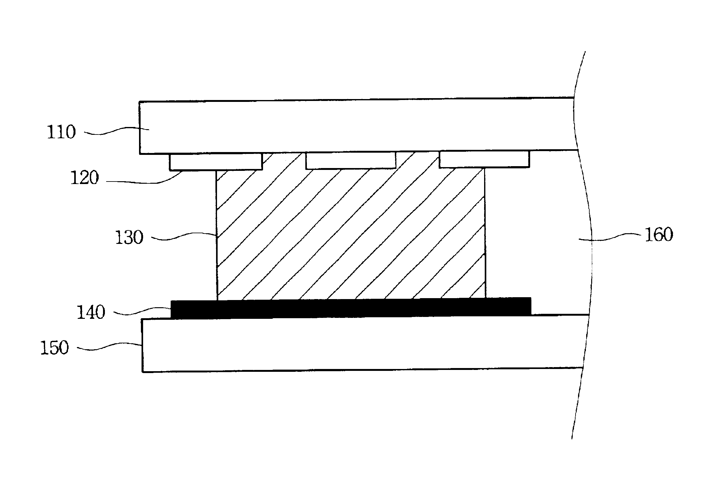
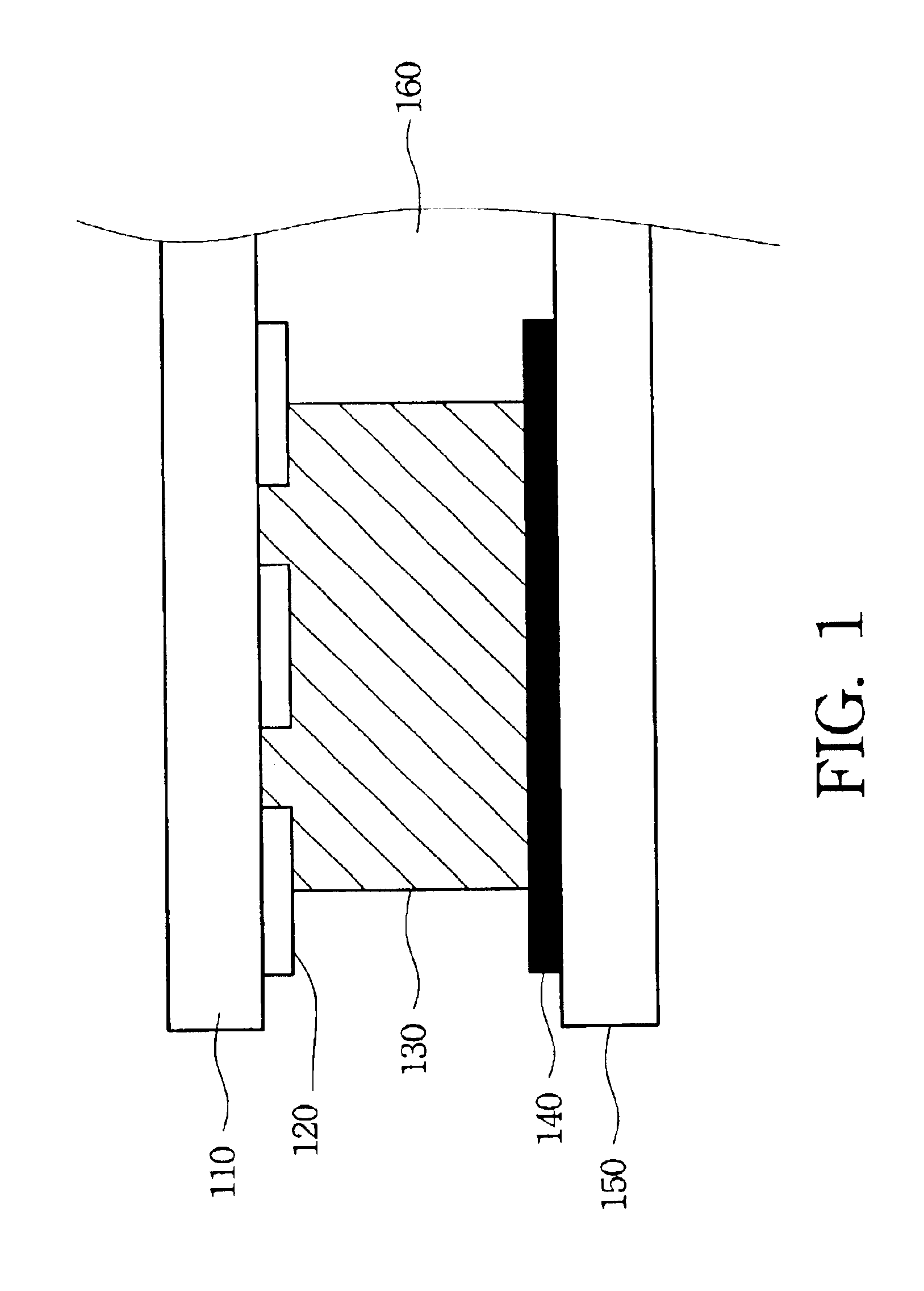
FIG. 1 shows a detailed cross-sectional view of a sealed position of a TFT-LCD according to the present invention. As the drawing shows, a TFT-LCD has a first substrate 110 and a second substrate 150, both of which are transparent glass material. Conventionally, the conductive pattern layer 120 is hidden behind the black matrix layer 140. The conductive pattern layer 120 includes peripheral driving circuits of the TFT-LCD. The peripheral driving circuits are formed by metal layers, made of copper, aluminun, or chromium, and positioned in a non-display area.

The TFT-LCD according to the present invention utilizes the ODF process to fill the LCD with LC. ...


PUM

PropertyMeasurementUnit
Timeaaaaaaaaaa
Structureaaaaaaaaaa
Electrical conductoraaaaaaaaaa

Abstract

A structure of liquid crystal display and manufacture method thereof are described. The liquid crystal display is manufactured by a one drop fill process. The display comprises a first substrate, a second substrate, a conductive pattern layer, a black matrix layer, a liquid crystal layer and an ultraviolet-type seal. The metal pattern layer is made of indium tin oxide and formed on the first substrate. Therefore, the metal pattern layer is a transparent layer allowing the ultraviolet light to pass through. The ultraviolet-type seal is pre-cured by the ultraviolet light from the first substrate direction to the seal, and then cured by a heating process. Hence, the liquid crystal pollution problem is reduced.

Description

FIELD OF THE INVENTIONThe present invention relates to a structure of a liquid crystal display and especially to a manufacture method of the liquid crystal display.BACKGROUND OF THE INVENTIONRecently, liquid crystal displays (LCD) have been widely applied in electrical products, due to the rapid progress of optical technology and semiconductor technology. Moreover, with the advantages of high image quality, compact size, light weight, low driving voltage, and low power consumption, LCDs have been introduced into portable computers, personal digital assistants, color televisions, and are gradually replacing the cathode ray tubes (CRT) used in conventional displays. LCDs are becoming the mainstream display apparatus.The main part of an LCD is a liquid crystal (LC) unit composed of two parallel transparent substrates and LC sealed therein. The main LCD trend is thin film transistor (TFT) LCDs. The fabrication processes of a TFT-LCD can be divided into four parts: TFT array process, col...

Claims


Application Information

Patent Timeline
IPC IPC(8): G02F1/13G02F1/1341G02F1/1339
CPCG02F1/1339G02F1/1341G02F2202/025G02F2202/023
Inventor LEE, YU-CHISHIH, PO-HSIU
Owner WUHAN CHINA STAR OPTOELECTRONICS TECH CO LTD
Features
  • R&D
  • Intellectual Property
  • Life Sciences
  • Materials
  • Tech Scout
  • Unparalleled Data Quality
  • Higher Quality Content
  • 60% Fewer Hallucinations
Learn More