Radio frequency module

a radio frequency module and radio frequency technology, applied in the direction of printed circuit aspects, basic electric elements, electrical apparatus construction details, etc., can solve the problems of increasing the cost of radio frequency modules. , to achieve the effect of reducing the thermal effect, reducing thermal interference, and increasing the integration

Inactive Publication Date: 2005-04-12
HITACHI LTD
View PDF8 Cites 39 Cited by
  • Summary
  • Abstract
  • Description
  • Claims
  • Application Information

AI Technical Summary

Benefits of technology

To put the first chip and the second chip at the different conductor layer each other is effective to reduce the thermal effect to the second chip, because the distance between the first chip and the second chip becomes longer than that in case of mounting them on the same layer.
According to the present invention, even when a first device which has a power amplifying function and a second device which has sensitive temperature dependence of characteristics such as a surface acoustic wave device (hereinafter referred to as a “SAW” device) are integrated on a substrate, the temp

Problems solved by technology

PA requires a heat dissipation structure because it consumes much electric power and generates heat.
However, these conventional techniques have the following drawback: in a module which integrates a power amplifier and a device whose operating characteristics vary with rise in temperature, namely a device having sensitive temperature dependence of characteristics, on a substrate, the influence of the heat generated by the PA on the device having sensitive temperature dependence of characteristics is not taken into consideration, or though it is taken into consideration to mount a PA and a device having sensitive temperature depe

Method used


Image

  • Radio frequency module
  • Radio frequency module
  • Radio frequency module

Examples


seventh embodiment

FIG. 12 shows the present invention.

eighth embodiment

FIG. 13 shows the present invention.

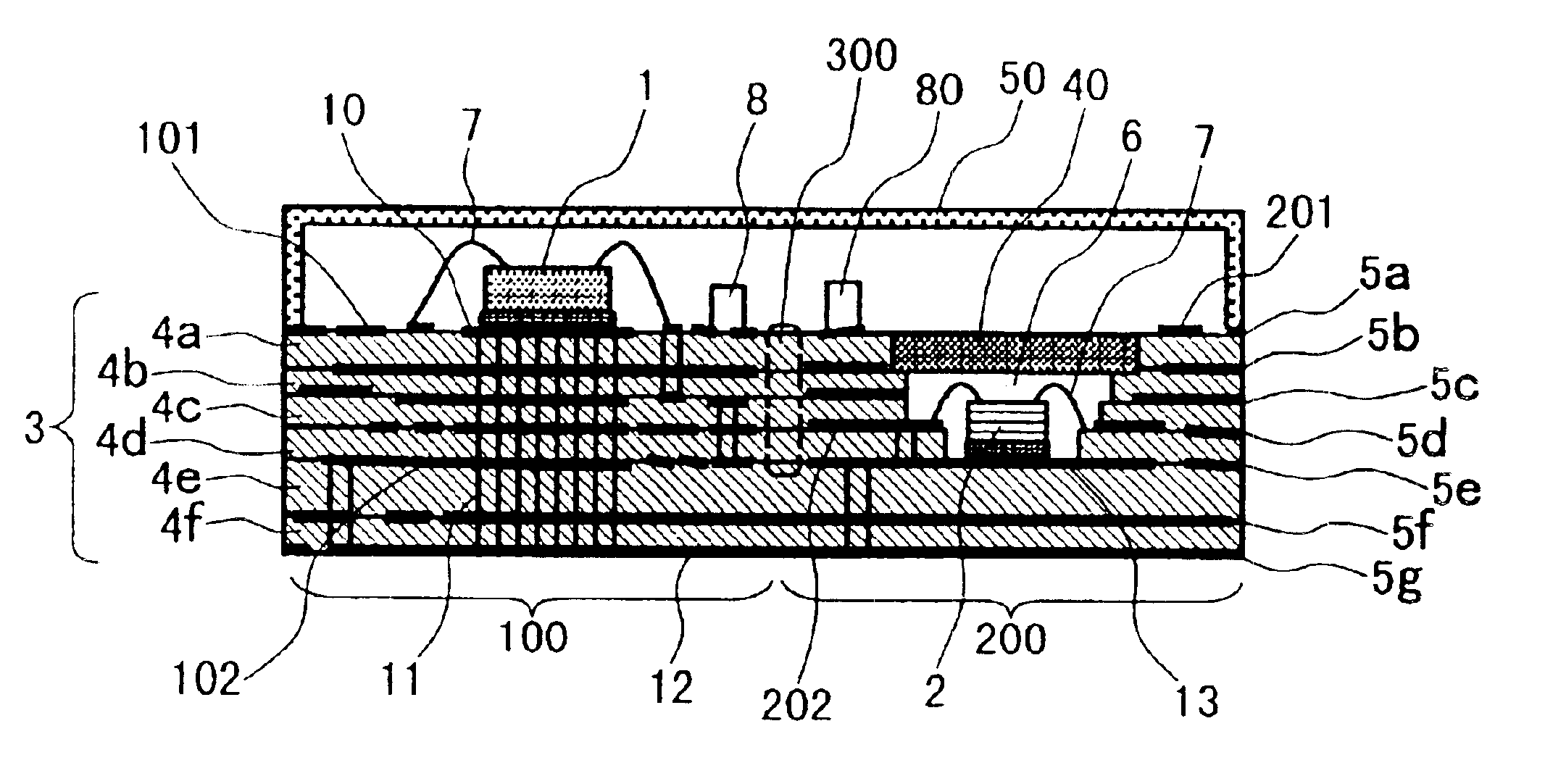
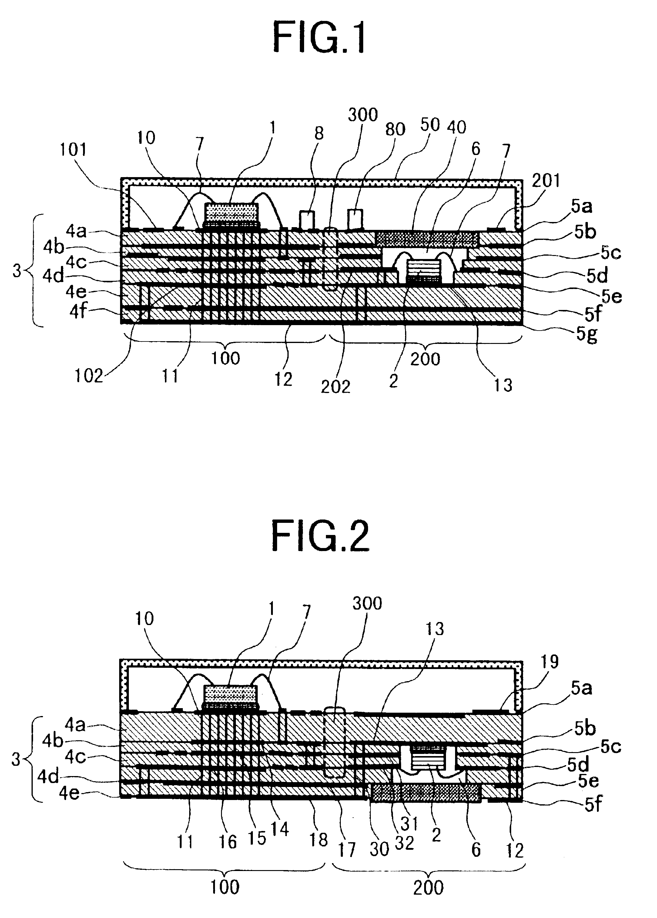
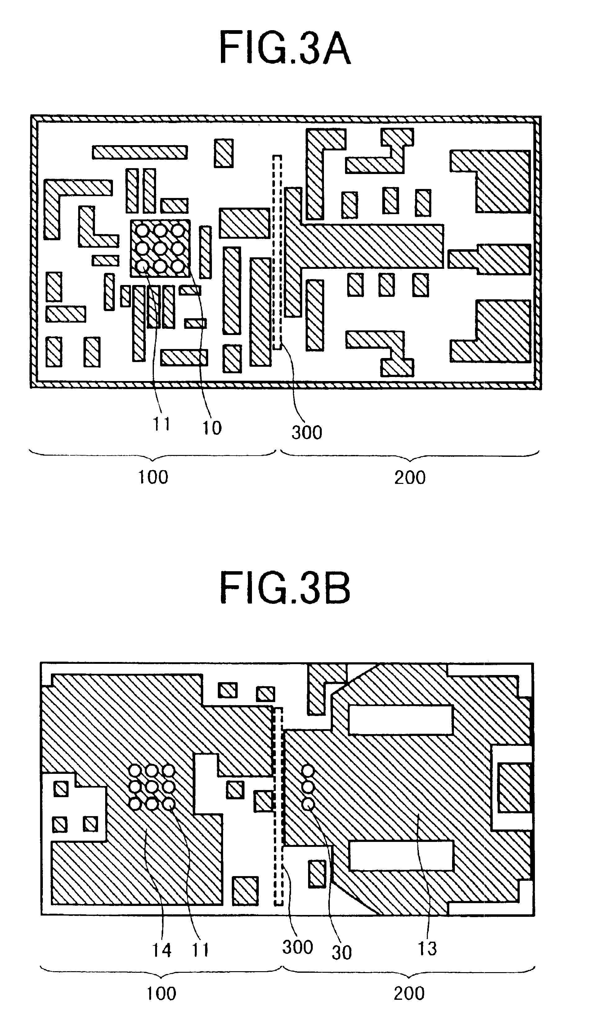
FIGS. 12 and 13 only show the shape of the multilayer substrate 3 and the positional relationship between the power amplifier 1 and the SAW device 2 where the conductor patterns of the radio frequency module are omitted. Here, the conductor patterns on the respective layers are much the same as those in the embodiments mentioned earlier. In these embodiments, the power amplifier 1 is located on the top face of the multilayer substrate 3 and the SAW device 2 is located inside the cavity 6 made through the bottom of the substrate 3. The multilayer substrate 3 is mounted on the motherboard 350.

In these embodiments, top view of the substrate of the radio frequency module is not rectangular but L-shaped or U-shaped and the power amplifier 1 and the SAW device 2 are located in the peripheral area of the module as illustrated in FIGS. 12 and 13. The module structures according to these embodiments make it possible to increase the distance between the pow...


PUM


Abstract

In a compact radio frequency module, a first chip forms a heater element and a second chip forms a device whose operating characteristics vary with temperature change or whose maximum operating temperature is lower than the maximum operating temperature of the first chip. A multilayer substrate has a plurality of dielectric layers and a plurality of conductor layers and mechanically supports the firs chip and the second chip with some of the conductor layers electrically connected with these chips. The module can conduct the heat generated by the first chip throughout the module; guide the heat generated by the first chip from the module's top face side to its bottom face side; and interrupt the heat conduction from the first conductor pattern on which the first chip is placed to the second conductor pattern on which the second chip is placed.

Description

BACKGROUND OF THE INVENTION1. Field of the InventionThe present invention relates to wireless communications and particularly to radio frequency components for use in mobile communication terminals such as mobile phones and wireless communication terminals such as wireless LAN, which feature increased function, high integration, reduced size and low price.2. Description of the Related ArtWith the growing tendency towards more compact wireless communication terminals, there is demand for radio frequency components for wireless communication terminals that fit into a smaller packaging area. Conventionally, circuit of radio frequency parts have been divided into several blocks by function and the blocks have been manufactured separately as modules while efforts have been made to improve reliability, reduce size and increase integration for each module. For example, methods of heat dissipation in power amplifier (hereinafter referred to as PA) modules including power amplifiers as heate...

Claims


Application Information

Patent Timeline
IPC IPC(8): H01L23/34H05K1/02H05K1/00H05K1/03H01L23/12H01L23/367H01L25/04H01L25/18
CPCH01L23/345H05K1/0201H01L23/3677H01L2924/16251H05K1/0206H05K1/0298H05K1/0306H05K2201/062H01L2224/32225H01L2224/48227H01L2224/73265H01L2924/19105H01L2924/15153H01L2924/15313H01L2924/00012H01L2224/48091H01L24/73
Inventor TAKEDA, ERIKOISOBE, ATSUSHITANAKA, SATOSHIOKABE, HIROSHI
Owner HITACHI LTD
Why Eureka
Try Eureka