

Current drive circuit avoiding effect of voltage drop caused by load and semiconductor memory device equipped therewith
a current drive circuit and load technology, applied in semiconductor devices, digital storage, instruments, etc., can solve the problems of driver transistor leakage current, and the inability to increase the drivability of the current drive circuit, so as to achieve the effect of decreasing the drive curren
- Summary
- Abstract
- Description
- Claims
- Application Information
AI Technical Summary
Benefits of technology
Problems solved by technology
Method used
Image

Examples
first embodiment
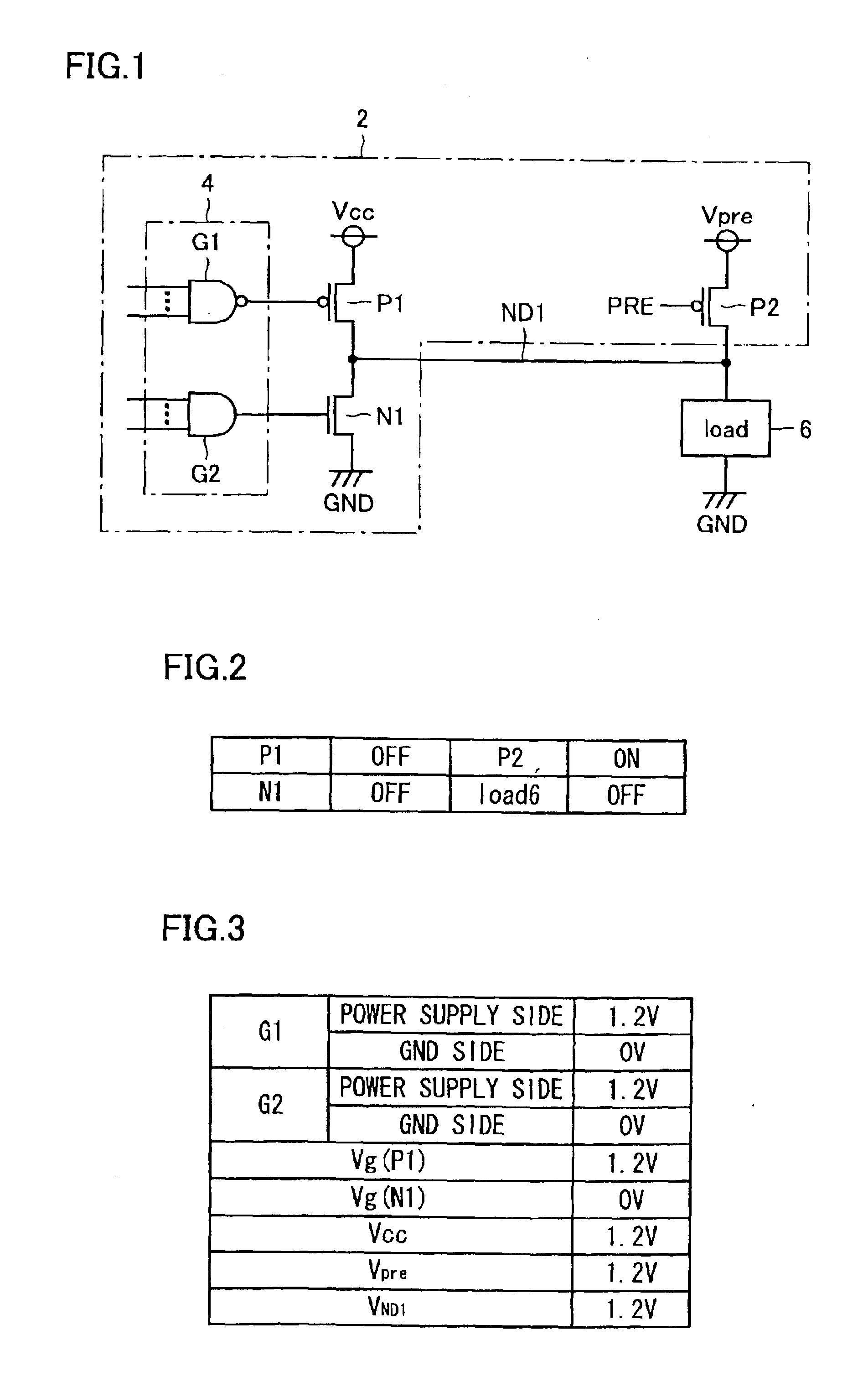
FIG. 1 is a circuit diagram showing the configuration of a current drive circuit according to a first embodiment of the present invention. Referring to FIG. 1, current drive circuit 2 includes P-channel MOS transistors P1, P2, an N-channel MOS transistor N1, a gate potential control circuit 4, power supply nodes Vcc, Vpre, and a ground node GND. Gate potential control circuit 4 includes an NAND gate G1 and an AND gate G2.
P-channel MOS transistor P1 and N-channel MOS transistor N1 (hereinafter also referred to as “driver transistor”) are configured with gate insulating films thinner than a gate insulating film of a driver transistor in a conventional current drive circuit. P-channel MOS transistor P1 is connected between node ND1 connected to a load circuit 6 and power supply node Vcc, and receives an output signal from NAND gate G1 at its gate. N-channel MOS transistor N1 is connected between node ND1 and ground node GND, and receives an output signal from AND gate G2 at its gate. N...
second embodiment
In a second embodiment, the current drive circuit described in the first embodiment is applied to MRAM device.
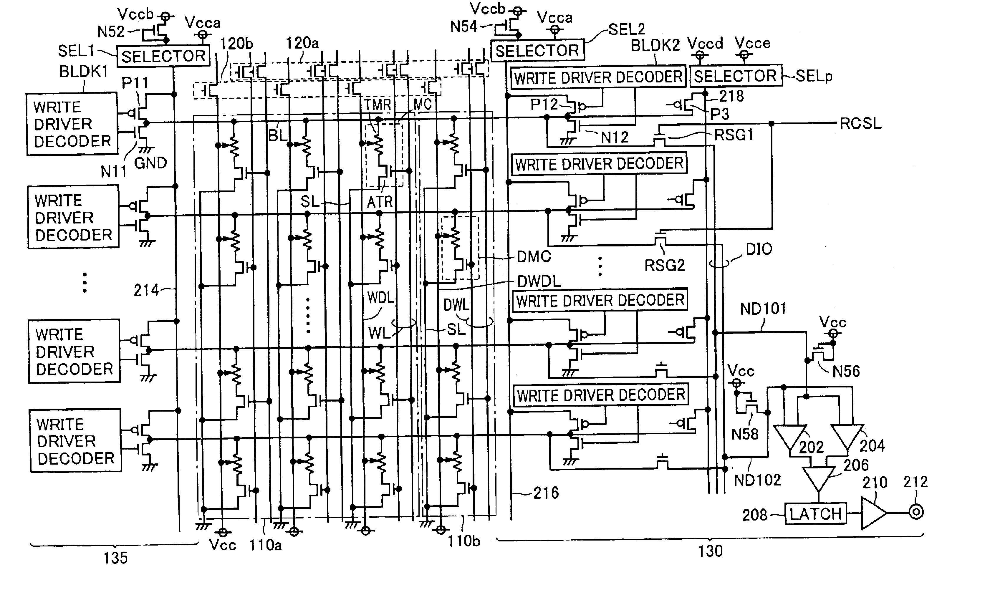
FIG. 8 is a schematic block diagram showing the overall configuration of MRAM device according to the second embodiment the present invention. Referring to FIG. 8, MRAM device 100 performs random access in response to control circuit CMD and address signal ADD from the outside, and performs writing of input data DIN to, or reading of output data DOUT from, a memory cell selected as the subject of data reading / writing (hereinafter also referred to as “select memory cell”).
MRAM device 100 includes a control circuit 105 controlling the overall operation of MRAM device 100 in response to control signal CMD, and a memory array 110 including memory cells MC arranged in rows and columns.
In memory array 110, word lines WL and write digit lines WDL are arranged corresponding to the rows of the memory cell, and bit lines BL and source lines SL are arranged corresponding to the columns...
third embodiment
In a third embodiment of the present invention, a current drive circuit in which driver transistor is configured with an N-channel MOS transistor will be described.
FIG. 22 is a circuit diagram showing the configuration of a current drive circuit according to a third embodiment.
Referring to FIG. 22, a current drive circuit 2A has the configuration of current drive circuit 2 according to the first embodiment, only that P-channel MOS transistor P1 is replaced by an N-channel MOS transistor N2, and gate potential control circuit 4 is replaced by gate potential control circuit 4A. Gate potential control circuit 4A has the configuration of gate potential control circuit 4, only that NAND gate G1 is replaced by an AND gate G3.
N-channel MOS transistor N2, similarly to N-channel MOS transistor N1 and P-channel MOS transistor P2, is configured with thin gate insulating film as compared to the gate insulating film of a driver transistor in a conventional current drive circuit. AND gate G3 outp...
PUM
 Abstract
Description
Claims
Application Information