FCSEL that frequency doubles its output emissions using sum-frequency generation

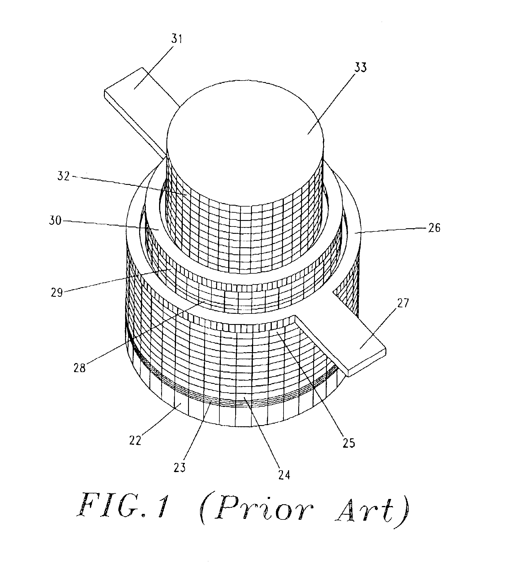
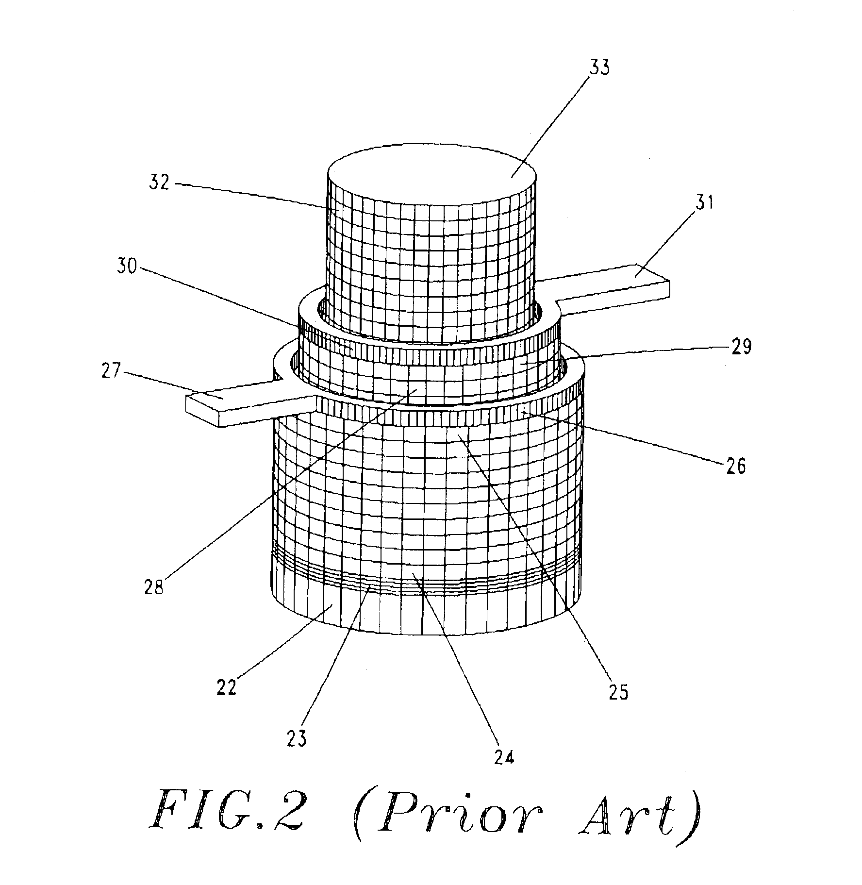
a semiconductor laser and sum-frequency generation technology, applied in semiconductor lasers, active medium materials, optical resonator shape and construction, etc., can solve the problems of difficult and costly phase-matching within birefringent crystalline materials, difficult and costly production of these materials, and the emission output is difficult to control

Inactive Publication Date: 2005-04-12
HENRICHS JOSEPH REID
View PDF25 Cites 43 Cited by
  • Summary
  • Abstract
  • Description
  • Claims
  • Application Information

AI Technical Summary

Problems solved by technology

It is, however, the large size of these solid-state lasers, being composed of multiple components, that makes their production very costly, and their emission output very difficult to control.
However, it is very difficult and costly to execute phase-matching within the birefringent crystalline materials; e.g., such as (LiNbO3) “Lithium-Niobium-Trioxide”, (KNbO3) “Potassium-Niobium-Trioxide”, (GaAs) “Gallium-Arsenide”, and / or (ZnSSe) “Zinc-Sulfur-Selenium”, while working with the micron-sized architectures of VCSEL and related laser-diode technologies.
However, the larger the device the greater is its cost of manufacturing, and since this type of laser comprises a multitude of components, it can become extremely difficult control; resulting in unstable second-harmonic emission.
In addition, other devices are well known, which extract a second harmonic from the end surface of what is normally striped GaAs or AlGaAs semiconductor lasers (see, e.g., N. Ogasawara, R. Ito, H. Rokukawa and W. Katsurashima: Jpn. J. Appl. Phys., Vol. 26 (1987) 1386), but the power of the fundamental wave occurring inside these devices is low due to a low end facet reflectivity.
Additionally, the absorption loss is also large due to a stripped-laser's long cavity.
These devices have even greater difficulty in achieving a phase-matching structure.
Consequently, these disadvantages make it impossible to generate the second-harmonic with high efficiency.
However, a device of the type disclosed in the above publication, the output power of the second harmonic was small, due to the fundamental emission being distributed over to wide a range, the condensing of the fundamental light was to difficult to achieve and therefore, at present the practical application for this device has yet to be realized.
Consequently, achieving single-mode operation in selectively oxidized VCSELs is a challenging task, because the inherent index confinement within these high-performance lasers is very large.
A disadvantage, however, of etched-surface relief is that it requires careful alignment to the oxide aperture and can increase the optical scattering loss of the fundamental transverse optical-mode, as manifested by the relatively low (i.e., less than 2.0-mW) single-mode output powers that have been reported.
Creating this structure, however, requires a detailed understanding of the oxidation process, and produces additional loss for the previously mentioned fundamental transverse optical-mode as well.
The problem, however, is that by using even-longer cavity spacers can introduce multiple longitudinal optical-modes (i.e., causing what is sometimes called spatial hole burning), but single-transverse-optical-mode operation up to nearly 7-mW has been demonstrated.
Nevertheless, under the present circumstances such devices can only be used upon cooling to extremely low temperatures and, therefore are impractical as light sources at a room temperature.
However, since the before mentioned LEDs produce non-coherent light emissions, which often display wide line-width properties, the more complex semiconductor lasers, over recent years, have become more widely used than the previously mentioned LEDs in the before mentioned field of optoelectronics.
The problem is that they will not presently operate at the room temperatures commonly used in every day life of human beings; therefore, they have no practical application in the real world (i.e., real world meaning a world outside an environmentally controlled laboratory environment).
Therefore, due to an increase in electric resistance, disadvantages such as a decrease in the power exhibited by the fundamental wave do not arise.

Method used


Image

  • FCSEL that frequency doubles its output emissions using sum-frequency generation
  • FCSEL that frequency doubles its output emissions using sum-frequency generation
  • FCSEL that frequency doubles its output emissions using sum-frequency generation

Examples


Embodiment Construction

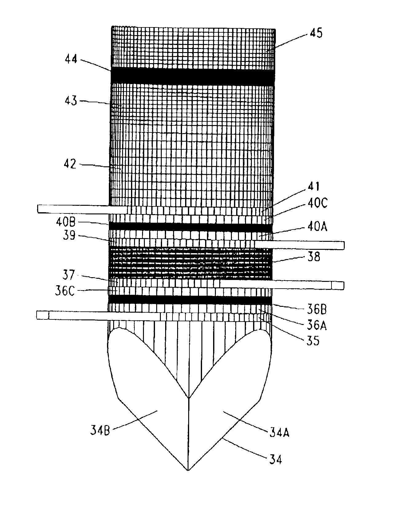
As a preferred embodiment of the present invention, a frequency-doubled sum-frequency generating FCSEL laser-diode, in contrast to the presented prior art, is constructed using compound semiconductor material that comprise various combinations of elements listed in columns III-V of the ‘Periodic Table of Elements’. For example, using a method of epitaxial deposition a compound semiconductor material such as GaAs, AlGaAs, GaInAsP, AlGaInP, GaInAsP, etc. may be utilized as construction material during the deposition of the present invention's active-regions.

Moreover, while a compound semiconductor material such as GaAs, GaAsP, etc., may be utilized as the semiconductor material that provides for a lattice matched substrate wafer. Further, a frequency-doubled sum-frequency generating FCSEL laser-diode will comprise a multitude of layered structures; e.g., a cavity, the reflectors, etc. Wherein, the multitude of layered structures are epitaxially deposited upon the top outermost surface...


PUM


Abstract

A “Folded Cavity Surface Emitting Laser” (FCSEL) sum frequency generating device capable of generating a second harmonic at room temperatures with high efficiency and output power, while having a small size, low energy consumption, and a low manufacturing cost. A FCSEL sum frequency generating semiconductor diode laser has a multilayered structure that comprises a mode discriminating polyhedral shaped prism waveguide, which is located at one end of two light emitting diodes, a partial photon reflecting mirror, which is located at the opposite end of the two light emitting diodes, and a phase-matching sum-frequency generating superlattice, which is located between the polyhedral shaped prism waveguide and the partial photon reflecting mirror.

Description

TECHNICAL FIELD OF INVENTIONThe present invention relates to semiconductor laser-diodes, or more specifically to frequency-doubled surface emitting semiconductor laser-diodes. Typically, these laser-diodes have multilayered vertically oriented optical cavity structures that comprise a substrate, a double-heterostructure (LED) “Light Emitting Diode”, a zinc-blend semiconductor material comprised superlattice, and two feedback providing contra-reflecting mirror structures. Further, these multilayered structures altogether are used to provide for an optical cavity capable of producing a frequency doubled laser emission output. More specifically, the present invention relates to a frequency-doubled (FCSEL) “Folded Cavity Surface Emitting Laser” that is capable of a highly efficient extraction of a second harmonic (i.e., especially monochromatic light, such as monochromatic violet, blue, or green light) in a predetermined direction perpendicular to a substrate.BACKGROUND OF THE INVENTION...

Claims


Application Information

Patent Timeline
Patent Type & Authority Patents(United States)
IPC IPC(8): H01S5/183H01S5/00H01L33/00H01S5/10H01S5/14H01L33/10
CPCH01S5/18341H01L33/105H01S5/0604H01S5/1085H01S5/426H01S5/18369H01S5/3215
Inventor HENRICHS, JOSEPH REID
Owner HENRICHS JOSEPH REID
Why Eureka
Try Eureka