Non-radiative dielectric waveguide and millimeter wave transmitting/receiving apparatus

a dielectric waveguide and millimeter wave technology, applied in the direction of waveguides, electrical devices, coupling devices, etc., can solve the problems of increasing the bonding area, and achieve the effects of reducing the loss of high-frequency signal transmission, excellent reliability, and reducing the radius of curvatur

Inactive Publication Date: 2005-04-19
KYOCERA CORP
View PDF14 Cites 8 Cited by
  • Summary
  • Abstract
  • Description
  • Claims
  • Application Information

AI Technical Summary

Benefits of technology

[0014]The invention has been made in view of the above-described problems, and accordingly its object is to provide a high-performance NRD guide which offers excellent reliability and suffers little from high-frequency signal transmission loss, and in which, since conversion of an electromagnetic wave of an LSM mode into an LSE mode is minimized, a sharp curved portion capable of dealing with a wide...

Problems solved by technology

Thus, when one surface of the dielectric strip facing to the parallel planar conductor is bonded to the paralle...

Method used


Image

  • Non-radiative dielectric waveguide and millimeter wave transmitting/receiving apparatus
  • Non-radiative dielectric waveguide and millimeter wave transmitting/receiving apparatus
  • Non-radiative dielectric waveguide and millimeter wave transmitting/receiving apparatus

Examples


example 1

[0126]An NRD guide S1 as shown in FIG. 1 was constructed as follows. As materials for the dielectric strip 2, ceramics with varying composition ratios were prepared that include a complex oxide comprising Mg, Al and Si as a main component. Their relative dielectric constants and Q values at a frequency of 60 GHz will be shown in Table 1.

[0127]

TABLE 1RelativeComposition (mol %)dielectricQ valueMgOAl2O3SiO2Additive(wt %)constant(60 GHz)155540Yb2O3106.85202101080Yb2O3104.814003103060Yb2O3155.818204104050Yb2O30.15.818505153550Yb2O355.62121617.517.565Yb2O354.820407204040Yb2O355.61010822.222.255.6——4.728109251758Yb2O3105.1249010252748Yb2O3105.627701125.53044.5Yb2O3105.8212012301060Yb2O355.2150013303040Yb2O355.6250014352045Yb2O3106.0206015353530Yb2O30.15.8208016401050Yb2O3105.8199017402040Yb2O355.5102018404020Yb2O3106.0147019405010Yb2O357.952020581032Yb2O357.512502122.222.255.6Yb2O30.14.829102222.222.255.6Yb2O314.826702322.222.255.6Yb2O354.827502422.222.255.6Yb2O374.930102522.222.255.6Yb2O...

example 2

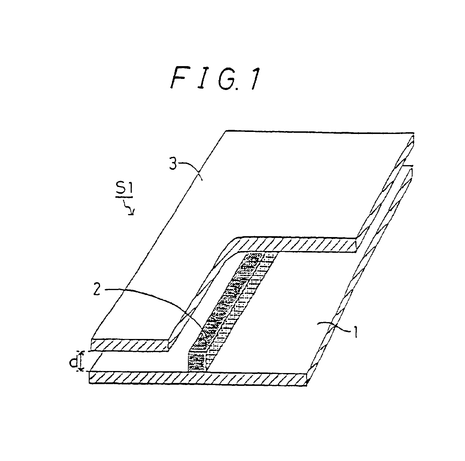
[0130]A pair of parallel planar conductors 1 and 3, each of which is made of an aluminum metal plate which is 80 mm long, 80 mm wide, and 2 mm in thickness, were arranged in parallel at a distance d of 1.8 mm. A dielectric strip 2 made of the cordierite ceramics as numbered 24 in Table 1 was placed between the parallel planar conductors 1 and 3. The sectional configuration of the dielectric strip 2 assumes a rectangular shape with a height of about 1.8 mm and a width of about 0.8 mm. The dielectric strip 2 had an open pore ratio of 0.5%. The surface roughness of the inner surface of the metal plate was measured by using a tracer-type surface roughness measuring machine, and the result was 0.3 μm. The metal plate and the dielectric strip 2 were bonded together with one-component epoxy resin. Transmission loss in high-frequency signals was measured by a network analyzer at a frequency of 76.5 GHz, and the result was 0.18 dB / cm. This means that the transmission loss is sufficiently sma...

example 3

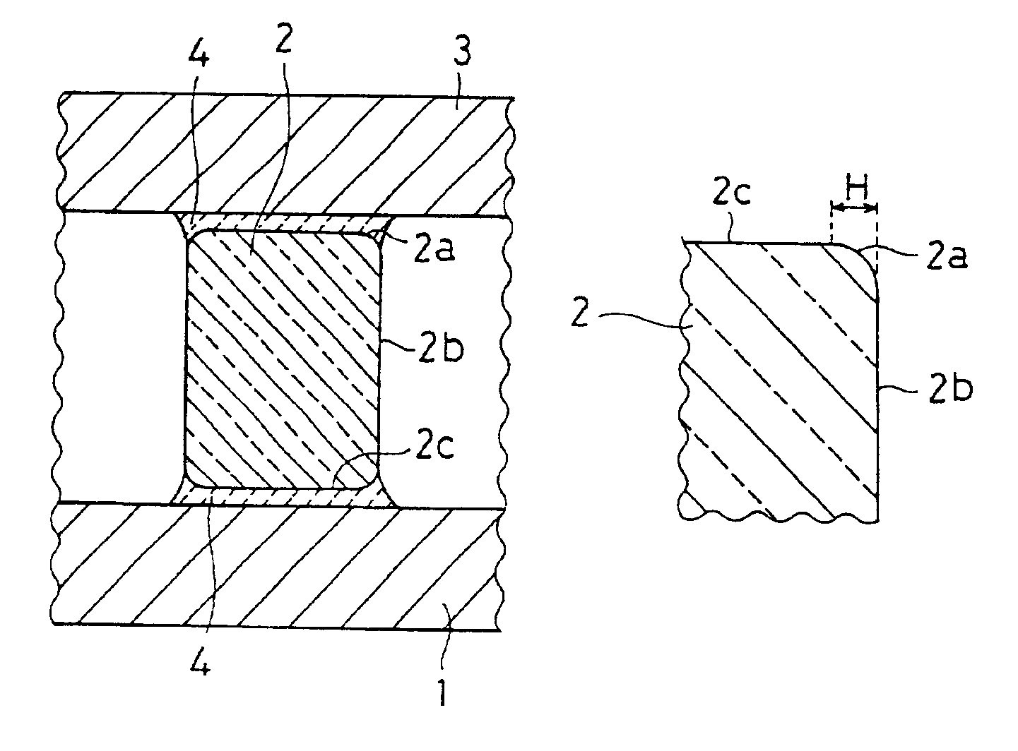
[0132]Another NRD guide S1 as shown in FIG. 1 was constructed basically in the same manner as in Example 1 except that, in the former, at each edge portion of the dielectric strip 2 is formed a chamfer 2a forming a plane and having a width H of 0.1 mm with respect to the faces 2c opposing to the parallel planar conductors, and a width H1 of 0.05 mm with respect to the side faces 2b (H>H1), as shown in FIG. 7C. Transmission loss in high-frequency signals was measured and the result was 0.16 dB / cm, which means that the transmission loss is sufficiently small in practice.


PUM


Abstract

The invention provides a highly-reliable, low-loss non-radiative dielectric waveguide. According to one aspect of the invention, a non-radiative dielectric waveguide comprises parallel planar conductors arranged at an interval of half or below of a high-frequency signal wavelength, and a dielectric strip interposed between the parallel planar conductors. The dielectric strip has a 0.01 to 0.3 mm-wide chamfer formed at its edge portion in a high-frequency signal transmission direction. According to another aspect of the invention, a non-radiative dielectric waveguide comprises parallel planar conductors arranged at an interval of half or below of a high-frequency signal wavelength, and a dielectric strip interposed between the parallel planar conductors. The dielectric strip is made of a ceramics having an open pore ratio of 5% or less.

Description

BACKGROUND OF THE INVENTION[0001]1. Field of the Invention[0002]The present invention relates to a non-radiative dielectric waveguide used in a high-frequency band, such as a millimeter wave band, and more particularly to a non-radiative dielectric waveguide suitably used for a millimeter wave integrated circuit or the like. The invention also relates to a millimeter wave transmitting / receiving apparatus of non-radiative dielectric waveguide type, such as a millimeter wave integrated circuit or a millimeter wave radar module.[0003]2. Description of the Related Art[0004]A conventional non-radiative dielectric waveguide (hereafter referred to as an NRD guide) S11 is shown in FIG. 8. In the NRD guide S11 shown in FIG. 8, a dielectric strip 202 is interposed between a pair of parallel planar conductors 201 and 203 arranged at an interval d of λ / 2 or below of a wavelength λ of an electromagnetic wave (high-frequency signal) propagating through the air at the usage frequency. This arrange...

Claims


Application Information

Patent Timeline
IPC IPC(8): H01P3/16H01P3/00
CPCH01P3/165
Inventor OKAMURA, TAKESHIHIRAMATSU, NOBUKI
Owner KYOCERA CORP
Why Eureka
Try Eureka