Non-linear photonic switch

a non-linear, photonic switch technology, applied in the direction of instruments, optical elements, optical waveguide light guides, etc., can solve the problems of time-consuming or rigorous procedure for photonic crystal construction, gate signal contamination of output signal,

Inactive Publication Date: 2005-04-26
SURFACE LOGIX INC
View PDF5 Cites 13 Cited by
  • Summary
  • Abstract
  • Description
  • Claims
  • Application Information

AI Technical Summary

Benefits of technology

[0011]A photonic switch according to the present invention may be formed using one of a selected group of non-linear optical materials. Each of the materials within this group has a refractive index that demonstrates a substantial peak as a function of wavelength, where the peak occurs at a wavelength distinct from the wavelength of the input signal. The formation of a photonic switch according to the prese...

Problems solved by technology

Current photonic switches may also suffer interference effects between the input and gate signals that carry through to the output signal, so that t...

Method used


Image

  • Non-linear photonic switch
  • Non-linear photonic switch
  • Non-linear photonic switch

Examples


Embodiment Construction

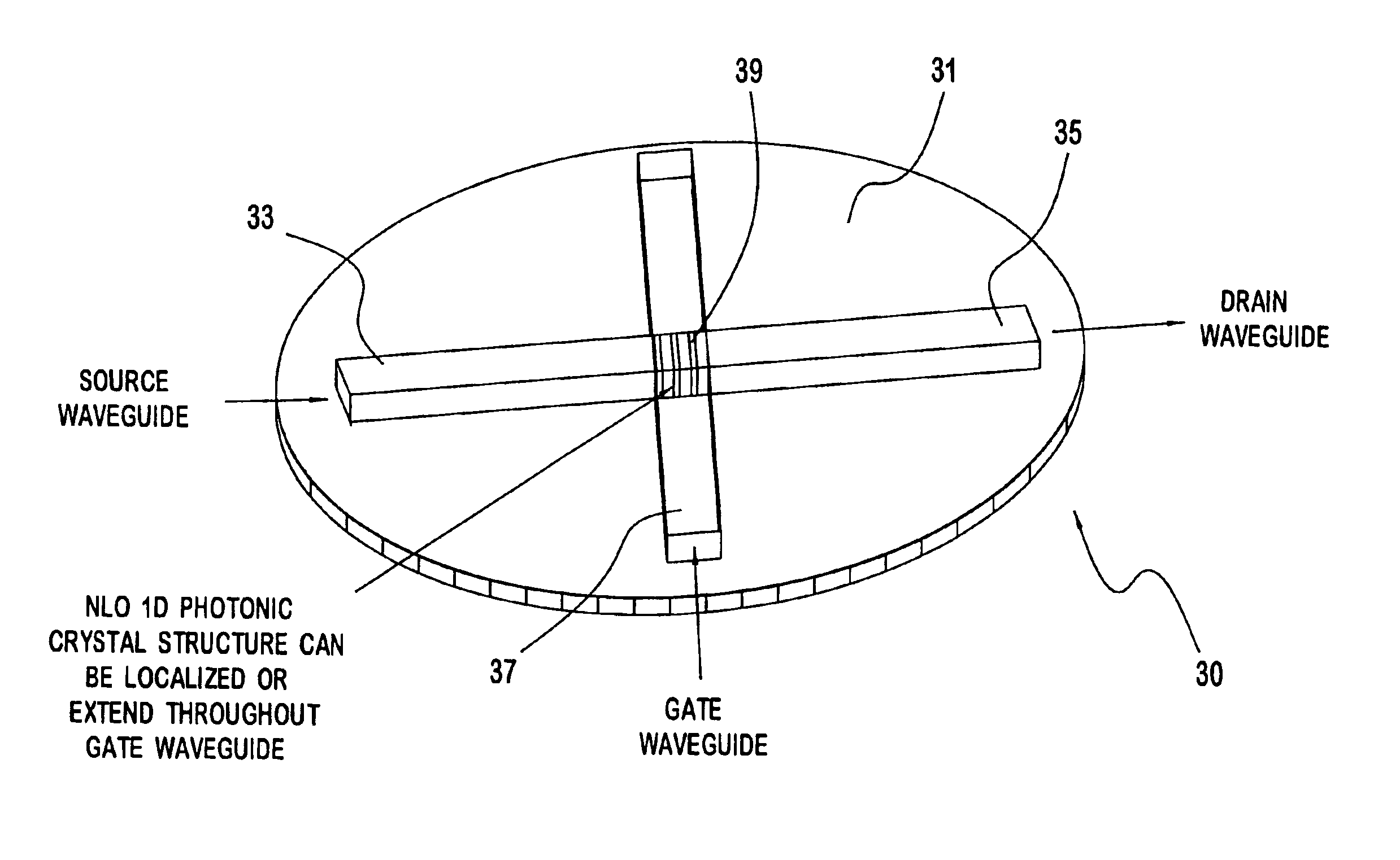
[0028]FIGS. 3 through 6 illustrate embodiments and features of a photonic switch according to the present invention. In general, a photonic switch 30 according to the present invention is illustrated schematically in FIG. 3, and could include any type of optical coupling, transistor, or the like. Photonic switches as described herein generally act on a source or input signal, using a gate signal, to influence or produce a given drain or output signal.

[0029]In the illustrated embodiment, photonic switch 30 includes a base wafer or substrate 31, which may be formed of any suitable material, for example silicon or glass. Source waveguide 33 and drain waveguide 35 are provided on opposite sides of photonic crystal 39. Source and drain waveguides 33, 35 are preferably formed from any suitable materials, for example silicon, silica, silicon oxynitride, cured sol-gel materials, UV curable polymers or other polymers. Photonic switch 30 also includes a gate waveguide 37 to provide a gate sig...


PUM


Abstract

A photonic switch may be formed using one of a selected group of non-linear optical materials. Each of the materials within this group has a refractive index that demonstrates a substantial peak as a function of wavelength. The photonic switch includes a positive gain, and thus acts as a photonic transistor. In addition, a photonic switch is formed so that a gate signal is applied in a direction that is substantially perpendicular to the direction of the input signal so that there is no effective contamination of the input signal by the gate signal affecting the output signal.

Description

RELATED APPLICATION(S)[0001]This application claims the benefit under 35 U.S.C. 119(e) of U.S. Provisional Application No. 60 / 331,283 filed Nov. 13, 2001, which is incorporated by reference herein.FIELD OF THE INVENTION[0002]The present invention relates to optical circuit devices, and in particular to optical or photonic switches made with a non-linear optical material, as well as methods of making such devices.BACKGROUND INFORMATION[0003]“Optical” or “photonic” switches allow selective transmission of electromagnetic signals, in particular the selective transmission of light. Photonic switches as used herein refers to any optical coupling or element having a source or input signal, an output or drain signal, and a third “gate” signal that affects the relationship between the source and gain signals. One such type of photonic switch is an optical transistor.[0004]In a known embodiment, an optical switch can be formed using a photonic crystal. FIGS. 1A, 1B and 1C illustrate known on...

Claims


Application Information

Patent Timeline
IPC IPC(8): G02F1/01G02F2/00G02B6/35G02B6/34G02B6/122G02F1/35G02F3/02
CPCB82Y20/00G02B6/1225G02F1/0126G02F2/004G02F3/024G02F1/3515G02F2202/32G02F2201/307
Inventor MCCOY, CHRISTOPHERCHEN, JOHN TSEN-TAO
Owner SURFACE LOGIX INC
Why Eureka
Try Eureka