Method for plasma etching a wafer after backside grinding

a plasma etching and backside technology, applied in the direction of basic electric elements, semiconductor/solid-state device manufacturing, electric devices, etc., can solve the problems of increased stress, uneven thickness of the wafer, and increased complexity of the photolithographic process required to define the circuit pattern, so as to prevent the non-uniform oxidation of the backside of the wafer

Inactive Publication Date: 2005-05-03
TAIWAN SEMICON MFG CO LTD
View PDF4 Cites 12 Cited by
  • Summary
  • Abstract
  • Description
  • Claims
  • Application Information

AI Technical Summary

Benefits of technology

[0018]The present invention is further directed to a method for preventing wafer backside non-uniform oxidation during a plasma ashing process for removing a photoresist layer which can be carried out by the steps of grinding a backside of a wafer exposing a bare silicon surface; oxidizing the bare silicon surface f...

Problems solved by technology

As the number of layers of metal interconnects increase, while the device geometry continuously decreases to allow more densely packed circuits, the photolithographic process required to define patterns of circuits becomes more complicated and difficult to carry out.
The silicon oxide layer formed along the peripheral edge of the...

Method used


Image

  • Method for plasma etching a wafer after backside grinding
  • Method for plasma etching a wafer after backside grinding

Examples


Embodiment Construction

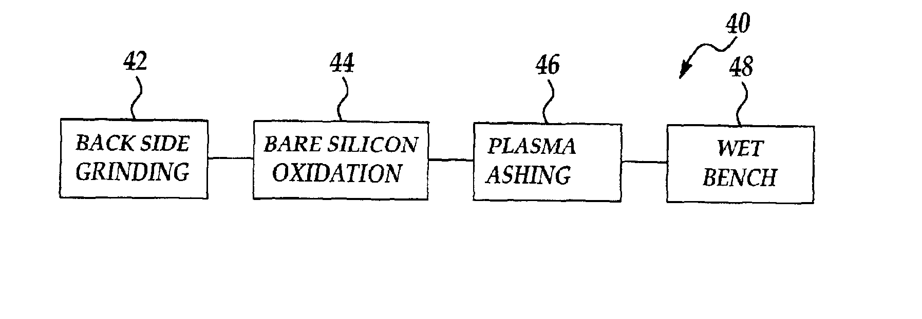
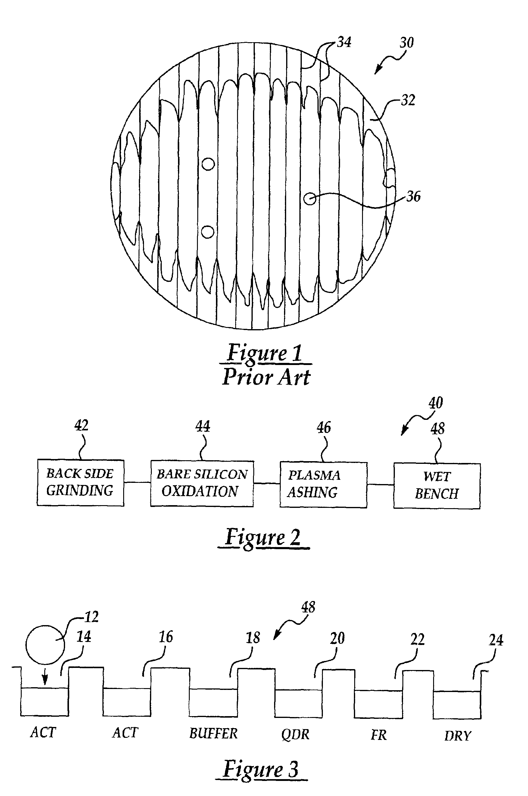
[0024]The present invention discloses a method for plasma etching a wafer after a backside grinding process is conducted that incorporates an oxidation pre-treatment step such that non-uniform formation of silicon oxide on the backside from the bare silicon can be avoided.

[0025]In the present invention novel method, a backside of a wafer is first ground to expose a bare silicon surface. The bare silicon surface is then oxidized to form a silicon oxide layer of at least 50 Å thick in an oxidation chamber. The wafer is then positioned in a plasma etch chamber with an active surface of the wafer exposed such that a surface layer can be plasma etched away from the active surface of the wafer. Optionally, the present invention method further includes the step of wet stripping in a wet bench process a residual surface layer away from the active surface of the wafer.

[0026]The oxidation step for oxidizing the bare silicon surface on the wafer backside can be carried out in an oxidation furn...


PUM


Abstract

A method for plasma etching a wafer after a backside grinding process which incorporates an oxidation pretreatment step is disclosed. The method includes the step of first grinding a backside of a wafer to expose a bare silicon surface. The bare silicon surface is then oxidized in an oxidation chamber to form a substantially uniform silicon oxide layer of at least 50 Å thick, and preferably at least 100 Å thick. The wafer is then positioned in a plasma etch chamber with an active surface of the wafer exposed, and a surface layer etched away by an oxygen plasma without causing any further silicon oxide formation on the backside of the wafer. The present invention novel plasma etching method can be advantageously used for removing an organic material layer, such as a photoresist layer from a wafer surface.

Description

FIELD OF THE INVENTION[0001]The present invention generally relates to a method for plasma etching a wafer surface for removing an unwanted coating layer and more particularly, relates to a method for plasma etching a photoresist layer from a wafer surface after a backside grinding of the wafer is performed without the non-uniform oxide layer formation defects.BACKGROUND OF THE INVENTION[0002]In the fabrication of semiconductor devices, various processing steps are started with a photolithographic process to first define a circuit on the wafer. For instance, in a modern memory device, multiple layers of metal conductors are required for providing a multi-layer metal interconnect structure. As the number of layers of metal interconnects increase, while the device geometry continuously decreases to allow more densely packed circuits, the photolithographic process required to define patterns of circuits becomes more complicated and difficult to carry out.[0003]After a process for formi...

Claims


Application Information

Patent Timeline
IPC IPC(8): H01L21/02H01L21/30H01L21/302H01L21/46H01L21/461
CPCH01L21/02054
Inventor CHANG, FENG-RULU, GAU-MINGCHANG, YEONG-RONG
Owner TAIWAN SEMICON MFG CO LTD
Why Eureka
Try Eureka