

BICMOS technology on SIMOX wafers
a technology of bicmos and wafers, applied in the direction of semiconductors, semiconductor devices, electrical equipment, etc., can solve the problems of affecting device performance, causing a lot of bumps, and rendering the resulting npn (or pnp) geometry non-planar, and achieving high current driverability, improved photolithography process, and low power consumption of soi technology
- Summary
- Abstract
- Description
- Claims
- Application Information
AI Technical Summary
Benefits of technology
Problems solved by technology
Method used
Image

Examples
Embodiment Construction
[0021]The invention and the various features and advantageous details thereof are explained more fully with reference to the non-limiting embodiments that are illustrated in the accompanying drawings and detailed in the following description. It should be noted that the features illustrated in the drawings are not necessarily drawn to scale. Descriptions of well-known components and processing techniques are omitted so as to not unnecessarily obscure the invention. The examples used herein are intended merely to facilitate an understanding of ways in which the invention may be practiced and to further enable those of skill in the art to practice the invention. Accordingly, the examples should not be construed as limiting the scope of the invention.
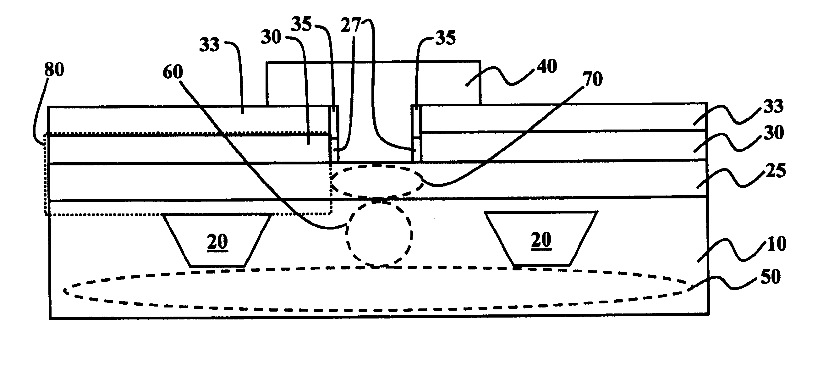
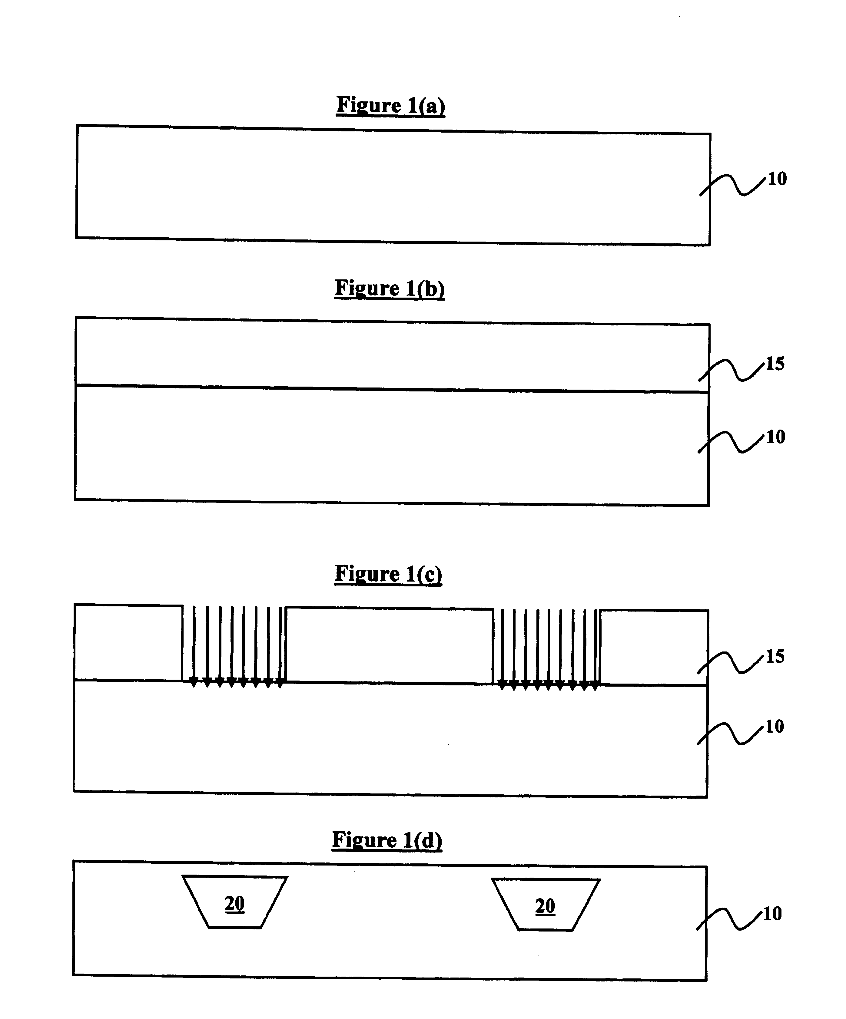
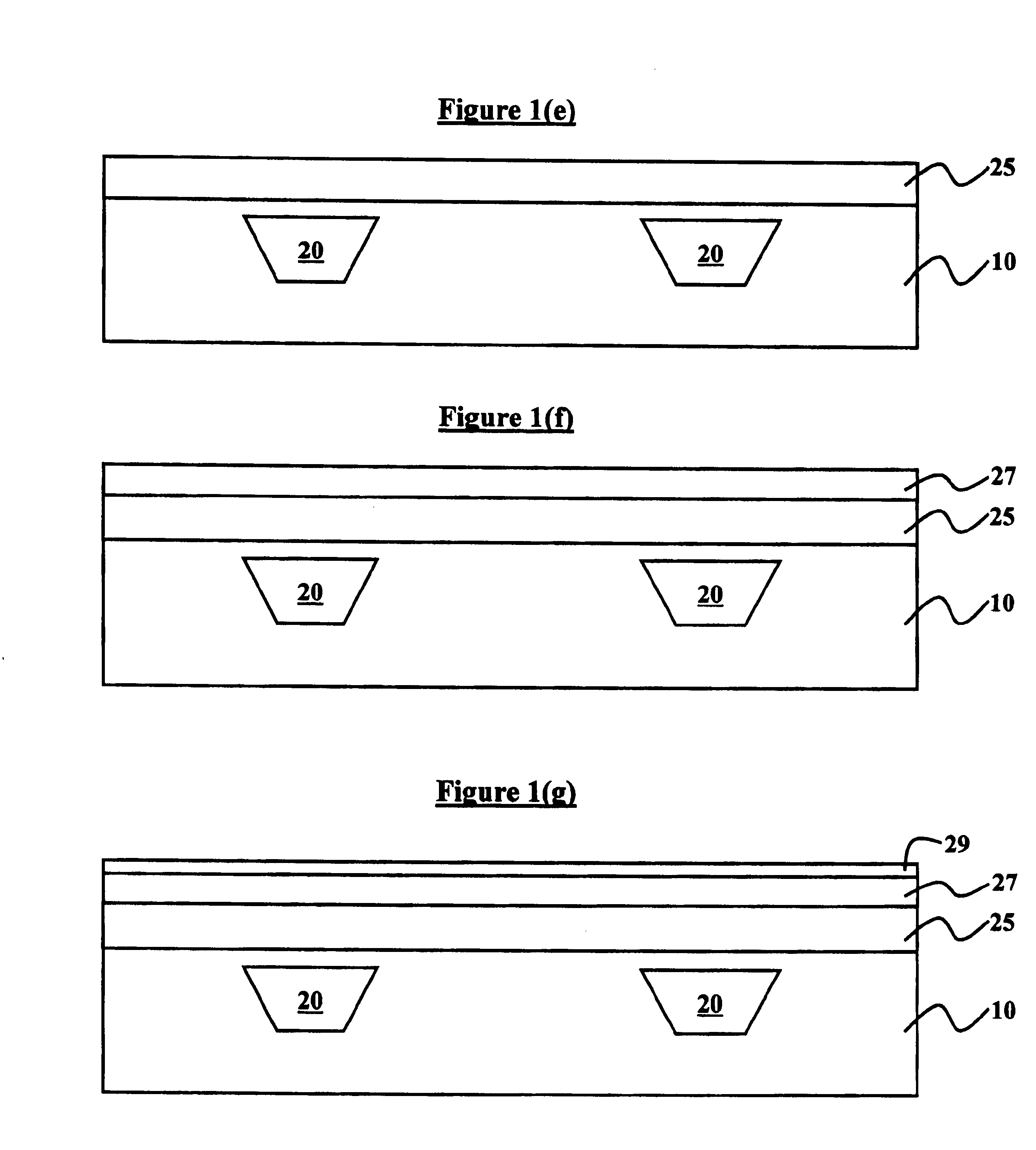
[0022]As previously mentioned, there is a need for a practical and simple device and methodology that integrates SiGe HBTs on SIMOX substrates and which overcomes the deficiencies of the conventional devices and methodologies. Referring no...
PUM
 Abstract
Description
Claims
Application Information