Dual gate dielectric scheme: SiON for high performance devices and high k for low power devices

a dielectric scheme and high-performance technology, applied in the field of semiconductor manufacturing, can solve the problems of large standby power consumption, inability to address the extendibility of gate dielectric thickness, and products with these devices commercially unacceptable, and achieve the effect of low cos

Inactive Publication Date: 2005-05-10
TAIWAN SEMICON MFG CO LTD
View PDF10 Cites 63 Cited by
  • Summary
  • Abstract
  • Description
  • Claims
  • Application Information

AI Technical Summary

Benefits of technology

[0013]A still further objective is to provide an efficient, low cost dual gate dielectric process in which the high k dielectric layer can be annealed simultaneously with the growth of the second dielectric layer.
[0014]These objectives are achieved by first providing a substrate with device areas separated by regions of insulating material such as STI features. In the first embodiment, an interfacial layer comprised of SiO2, SiON, or Si3N4 is deposited on the substrate. A high k dielectric material is then deposited by a chemical vapor deposition (CVD), metal-organic CVD (MOCVD), or atomic layer CVD (ALD) process. The high k dielectric material is selected from a group of metal oxides including Ta2O5, TiO2, Al2O3, ZrO2, HfO2, Y2O3, L2O3 and their aluminates and silicates. The high k dielectric material may comprise a single layer of one metal oxide or several layers including two or more metal oxides. A photoresist is coated and patterned on the high k dielectric layer to uncover the substrate in a region that will form the high performance device. After the high k dielectric and interfacial layers are removed in exposed regions, the photoresist is stripped and the substrate is cleaned. An ultra thin SiON layer with an EOT of preferably <10 nm is then deposited by using a silicon source gas in combination with NH3, NO or N2 with O2. During the deposition of the second dielectric layer, the high k dielectric layer is annealed in an in-situ process. A post-deposition anneal involving NH3 or a nitrogen containing gas may be added to further reduce leakage current and lower EOT. Conventional processing is followed to complete the construction of a MOSFET that is a low power device from the region containing the high k dielectric layer and a MOSFET that is a high performance device from the region containing the SiON dielectric layer.

Problems solved by technology

This will cause a large current in the standby mode (IOFF) and a large standby power consumption, thereby making products with these devices commercially unacceptable.
This prior art and the previous case do not address extendibility to gate dielectric thicknesses less than 20 Angstroms where high k dielectric materials will be needed.
However, the method does not teach how to form a dielectric layer for a high performance device and a high k dielectric layer for a low power device on the same substrate for a SOC application.

Method used


Image

  • Dual gate dielectric scheme: SiON for high performance devices and high k for low power devices
  • Dual gate dielectric scheme: SiON for high performance devices and high k for low power devices
  • Dual gate dielectric scheme: SiON for high performance devices and high k for low power devices

Examples


first embodiment

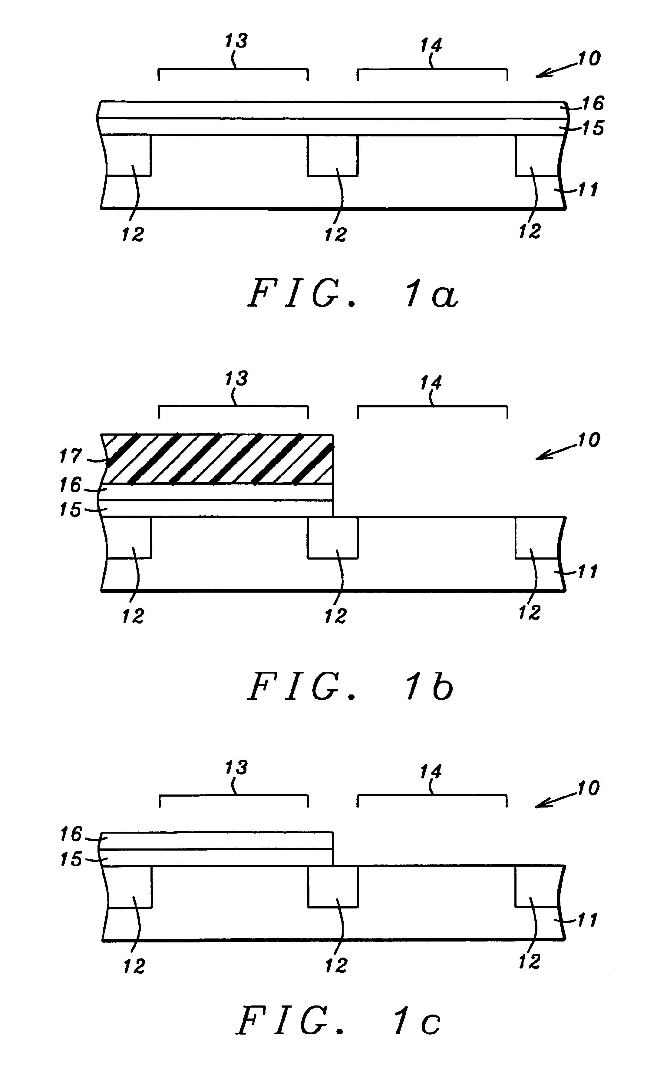
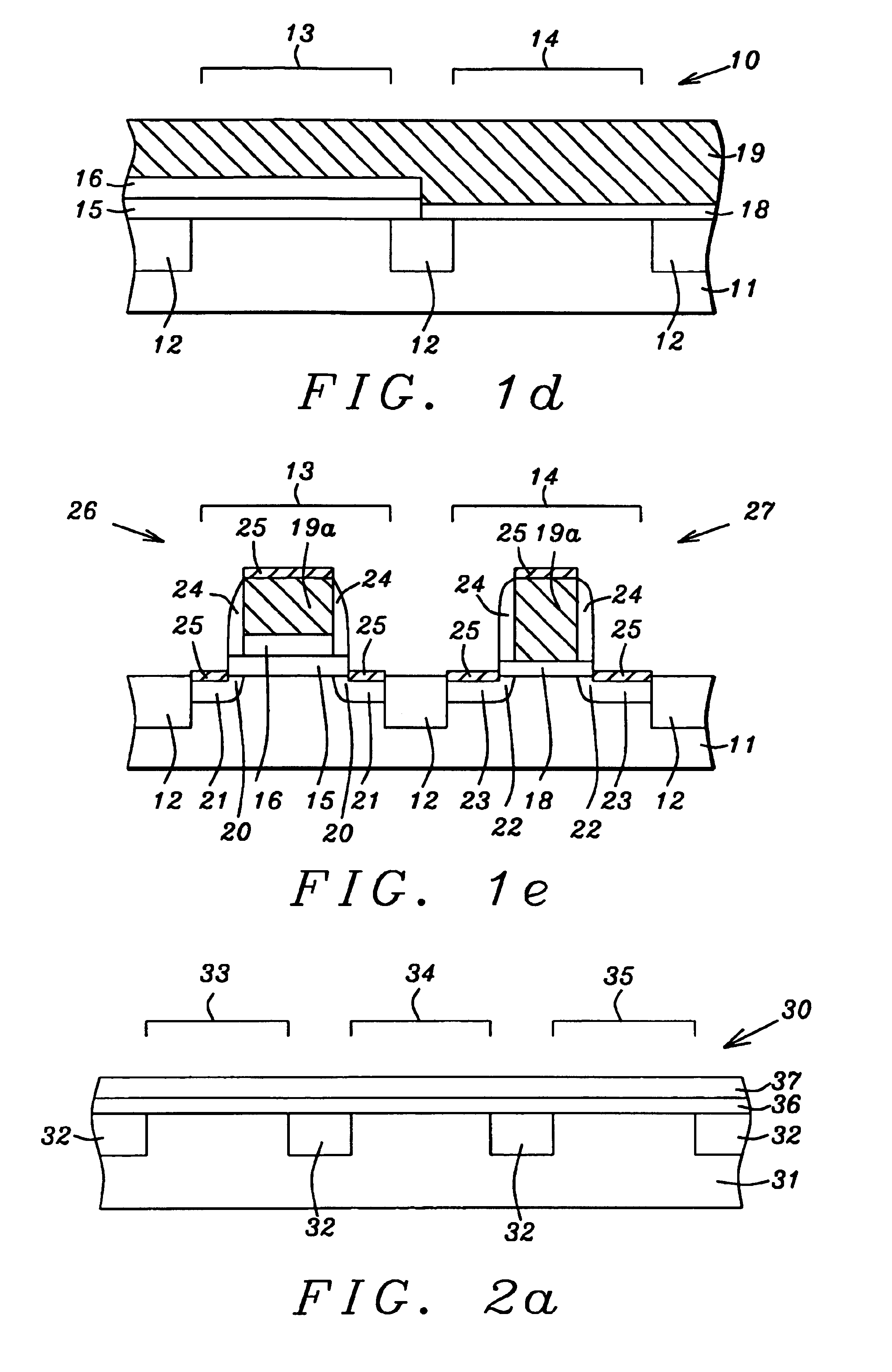
[0031]The present invention provides a method for forming a high k dielectric layer and an SiON dielectric layer on the same substrate. In the first embodiment, the high k dielectric layer is incorporated into a low power device and the SiON dielectric layer is incorporated into a high performance device.

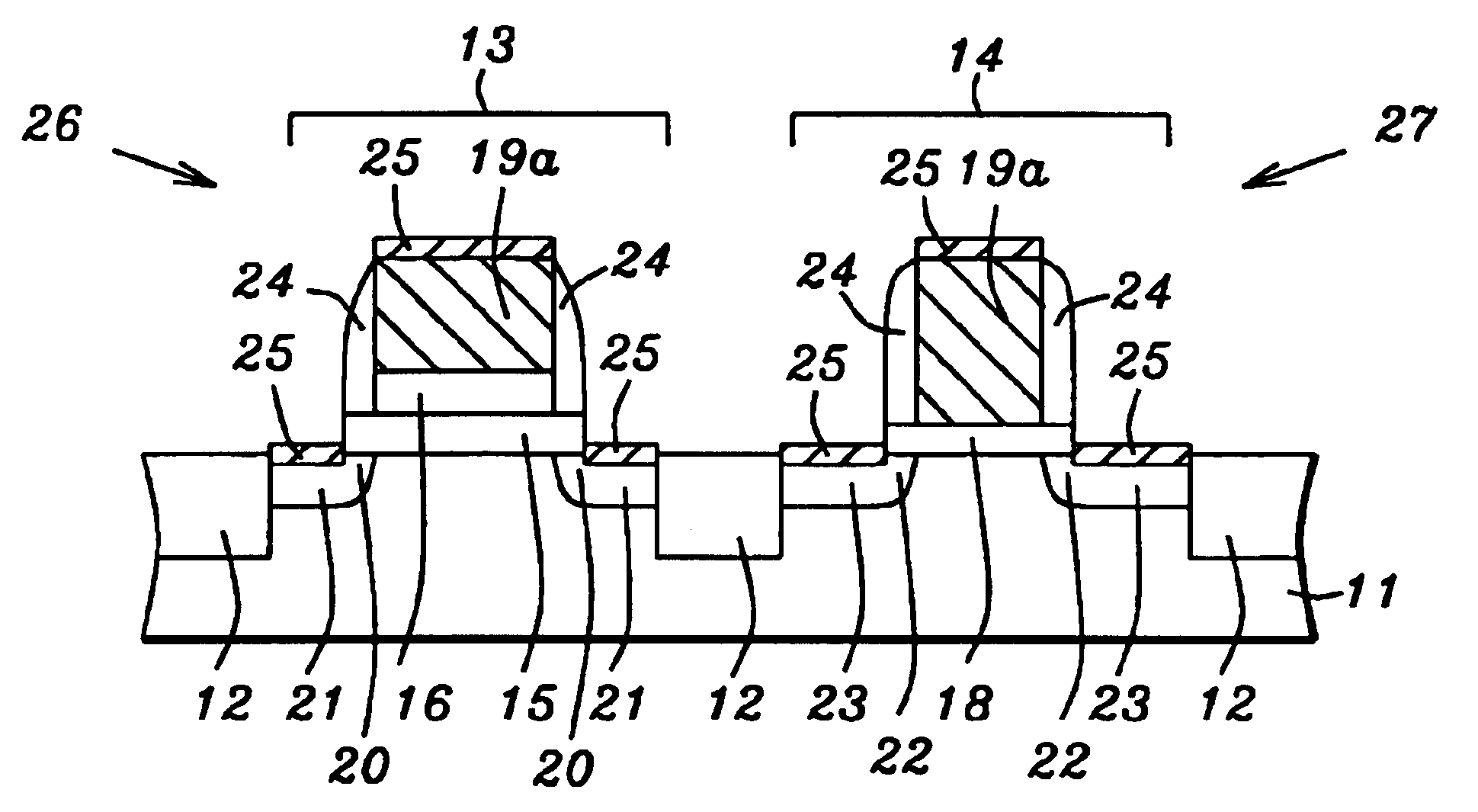
[0032]While the drawings in FIGS. 1a-1e are intended to give a description of the first embodiment, the scope of the present invention is not limited by the drawings. For example, the FIGS. 1a-1e are not necessarily drawn to scale. In addition, the substrate is simplified in the drawings and a substructure containing other devices and sub-layers is not shown. Referring to FIG. 1a, a structure 10 is shown which consists of a substrate 11 and shallow trench isolation regions 12 that separate device areas 13 and 14. A MOSFET which is a low power device will be fabricated or device area 13 and a MOSFET which is a high performance device will be fabricated on device area 14. The substrat...

second embodiment

[0057]An advantage of the second embodiment over prior art is that a device containing a high k dielectric layer which enables the low power device to meet future requirements of <1.8 nm EOT is formed on the same substrate with a high performance device having a gate dielectric EOT that is extendable to <1 nm for 50 nm and 70 nm technology nodes. Furthermore, an I / O device that provides greater SOC capability is also formed on the same substrate. Gate leakage current has been suppressed to an acceptable level in the low power device. The method can be readily implemented in a manufacturing scheme at a minimal cost, especially when the high k dielectric anneal step is performed in-situ with the deposition of the second gate dielectric layer.


PUM

PropertyMeasurementUnit
thicknessaaaaaaaaaa
thicknessaaaaaaaaaa
thicknessaaaaaaaaaa

Abstract

A method of forming dual gate dielectric layers that is extendable to satisfying requirements for 50 nm and 70 nm technology nodes is described. A substrate is provided with STI regions that separate device areas. An interfacial layer and a high k dielectric layer are sequentially deposited on the substrate. The two layers are removed over one device area and an ultra thin silicon oxynitride layer with an EOT<10 nm is grown on the exposed device area. The high k dielectric layer is annealed during growth of the SiON dielectric layer. The high k dielectric layer is formed from a metal oxide or its silicate or aluminate and enables a low power device to be fabricated with an EOT<1.8 nm with a suppressed leakage current. The method is compatible with a dual or triple oxide thickness process when forming multiple gates.

Description

[0001]This application is a continuation of U.S. Ser. No. 10 / 282,387, filed Oct. 29, 2002 now U.S. Pat No. 6,706,581.FIELD OF THE INVENTION[0002]The present invention relates to a method of semiconductor manufacturing. In particular, the method involves forming two or more gate dielectric layers comprised of different materials during the fabrication of integrated circuits for system on a chip (SOC) technology.BACKGROUND OF THE INVENTION[0003]Complimentary metal oxide semiconductor (CMOS) field effect transistor (FET) technology is being driven to smaller gate electrode sizes by a constant demand for higher performance. As stated in an article “Outlook on New Transistor Materials” by L. Peters in Semiconductor International, Oct. 1, 2001 edition, the next generation 70 nm and 50 nm technology nodes will need new gate dielectric materials in order to accommodate a shrinking gate size. A high k dielectric option comprised of a metal oxide is a leading candidate to replace the traditio...

Claims


Application Information

Patent Timeline
Patent Type & Authority Patents(United States)
IPC IPC(8): H01L21/8234
CPCH01L21/823456H01L21/823462
Inventor HOU, TOU-HUNGWANG, MING-FANGCHEN, CHI-CHUNYANG, CHIH-WEIYAO, LIANG-GICHEN, SHIH-CHANG
Owner TAIWAN SEMICON MFG CO LTD
Why Eureka
Try Eureka