Demodulating circuit and optical receiving circuit
a demodulating circuit and optical receiving circuit technology, applied in the field of demodulating circuits, can solve the problems of difficult dc potential compensation and rapid dc offset, and achieve the effect of mitigate the effect of dc offset variations
- Summary
- Abstract
- Description
- Claims
- Application Information
AI Technical Summary
Benefits of technology
Problems solved by technology
Method used
Image

Examples
first embodiment
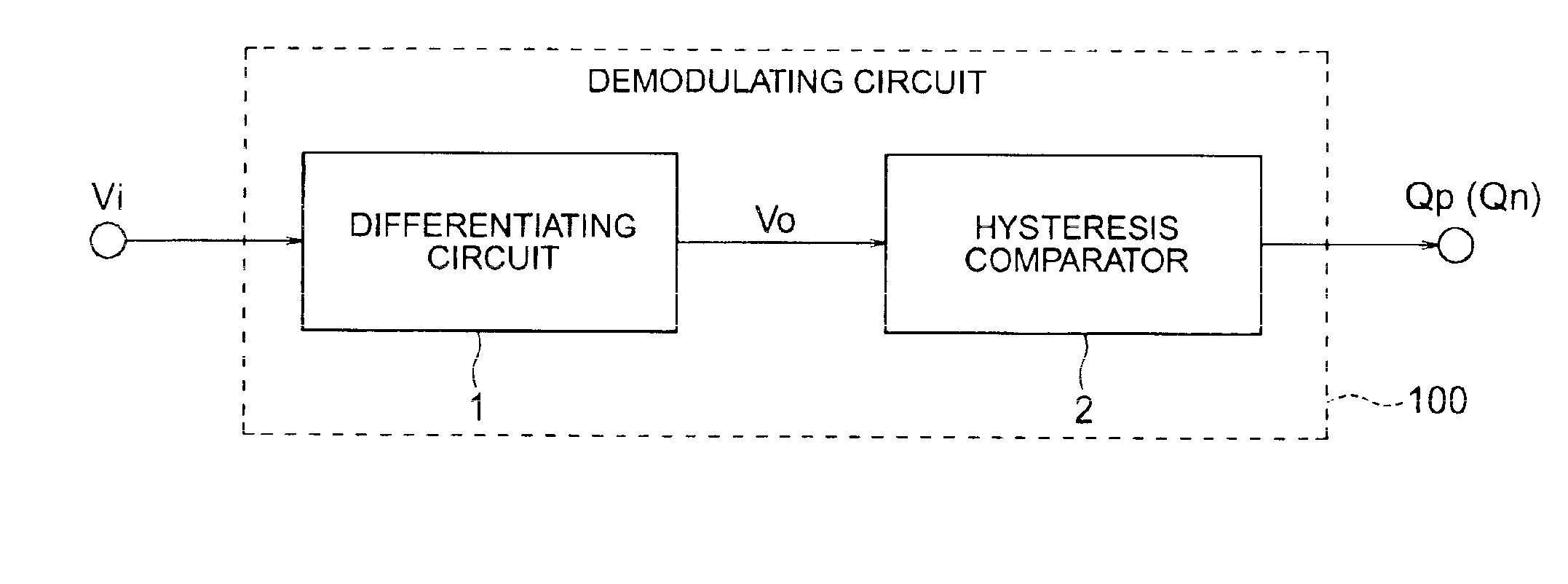
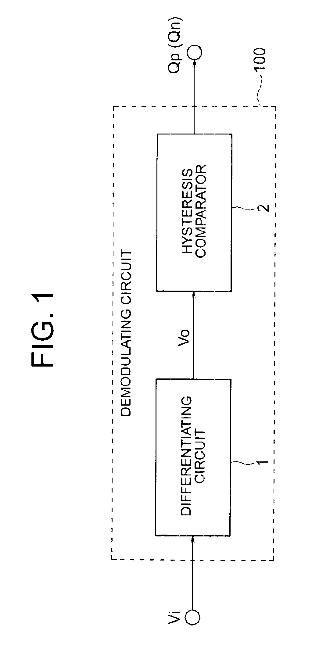
[0068]Referring to the block diagram in FIG. 1, the demodulating circuit 100 in the following embodiments receives a pulse signal Vi that may include runs of consecutive 1's or 0's of up to a specified length, demodulates the pulse signal Vi, and outputs a positive-phase demodulated signal Qp (and / or a negative-phase demodulated signal Qn) at prescribed high and low logic levels. The demodulating circuit 100 comprises a differentiating circuit 1 and a hysteresis comparator 2. The differentiating circuit 1 detects the change in voltage at the rise or fall of the input pulse signal Vi and generates a differentiated signal Vo corresponding approximately to the change. The hysteresis comparator 2 compares the differentiated signal Vo with a reference voltage Vr1 according to a pair of threshold voltages VothH and VothL, where VothH is higher than Vr1 and VothL is lower than Vr1. The hysteresis comparator 2 switches output states when Vo crosses these threshold voltage levels VothH and V...
second embodiment
[0093]FIG. 7 shows a demodulating circuit 100b in a second embodiment of the present invention. The second embodiment differs from the first embodiment in that the input pulse signal Vi is coupled to the inverting (−) input terminal of the comparator element 10 rather than the non-inverting (+) input terminal. For this reason, the demodulated signal Qn output from the hysteresis comparator 2b is inverted with respect to the input pulse signal Vi. Otherwise, the second embodiment is similar to the first embodiment.
[0094]The hysteresis comparator 2b in the demodulating circuit 100b includes the same comparator element 10 and resistance elements R1, R2 as in the first embodiment. The inverting (−) input terminal of the comparator element 10 receives a differentiated signal Vo; the non-inverting (+) input terminal receives a voltage related to the first reference voltage Vr1; the output terminal outputs a negative-phase demodulated signal Qn responsive to the voltage difference between ...
third embodiment
[0099]The block diagram in FIG. 8 shows the differentiating circuit 1c and hysteresis comparator 2c in a demodulating circuit 100c according to a third embodiment of the invention. The differentiating circuit 1c comprises an inverting amplifier 30 with a negative feedback resistance element Rf coupled between its input and output terminals. The inverting amplifier 30 receives the input pulse signal Vi via a differentiating capacitor Ct, and outputs a negative-phase differentiated signal Von. The hysteresis comparator 2c includes a comparator element 10, a first resistance element R1, and a second resistance element R2 as in the preceding embodiments. The comparator element 10 receives the negative-phase differentiated signal Von at its inverting (−) input terminal, and outputs a positive-phase demodulated signal Qp at the high or low logic level. The first resistance element R1 couples the positive-phase demodulated signal Qp to the non-inverting (+) input terminal of the comparator...
PUM
 Abstract
Description
Claims
Application Information
 - R&D
- Intellectual Property
- Life Sciences
- Materials
- Tech Scout
- Unparalleled Data Quality
- Higher Quality Content
- 60% Fewer Hallucinations
Browse by: Latest US Patents, China's latest patents, Technical Efficacy Thesaurus, Application Domain, Technology Topic, Popular Technical Reports.
© 2025 PatSnap. All rights reserved.Legal|Privacy policy|Modern Slavery Act Transparency Statement|Sitemap|About US| Contact US: help@patsnap.com