Method of preventing short circuits in magnetic film stacks

a technology of magnetic film and short circuit, which is applied in the direction of semiconductor devices, semiconductor/solid-state device details, electrical devices, etc., can solve the problems of difficult removal and tenacious conductive residue on the sidewalls of the film stack, and achieve the effect of preventing electrical short circui

Inactive Publication Date: 2005-05-17
APPLIED MATERIALS INC
View PDF17 Cites 37 Cited by
  • Summary
  • Abstract
  • Description
  • Claims
  • Application Information

AI Technical Summary

Benefits of technology

[0009]The disadvantages of the prior art are overcome by a method for preventing electrical short circuiting in a multi-layer magnetic film stack. The method comprises providing a film stack that includes a magnetic material that has an exposed surface. A protective layer is deposited on the ex

Problems solved by technology

Generally, the conductive residue that deposits on the sidew

Method used


Image

  • Method of preventing short circuits in magnetic film stacks
  • Method of preventing short circuits in magnetic film stacks
  • Method of preventing short circuits in magnetic film stacks

Examples


Embodiment Construction

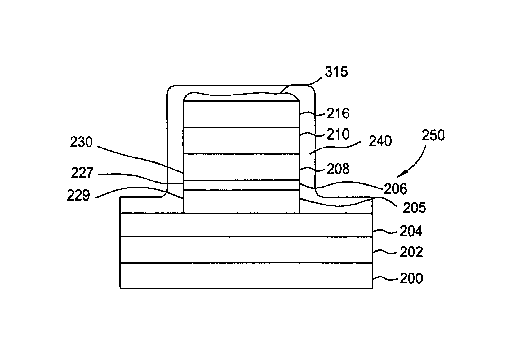
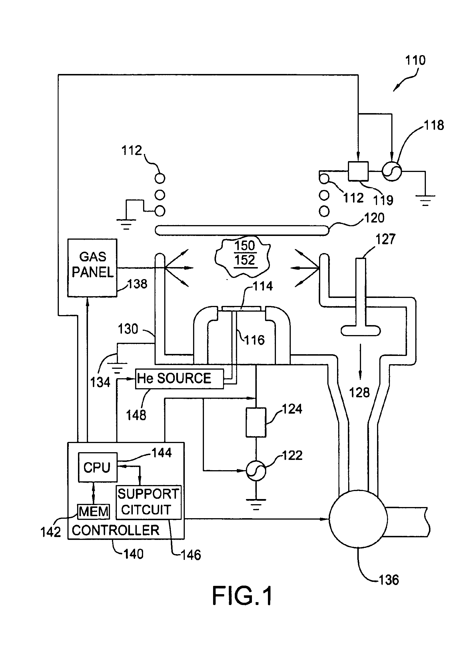
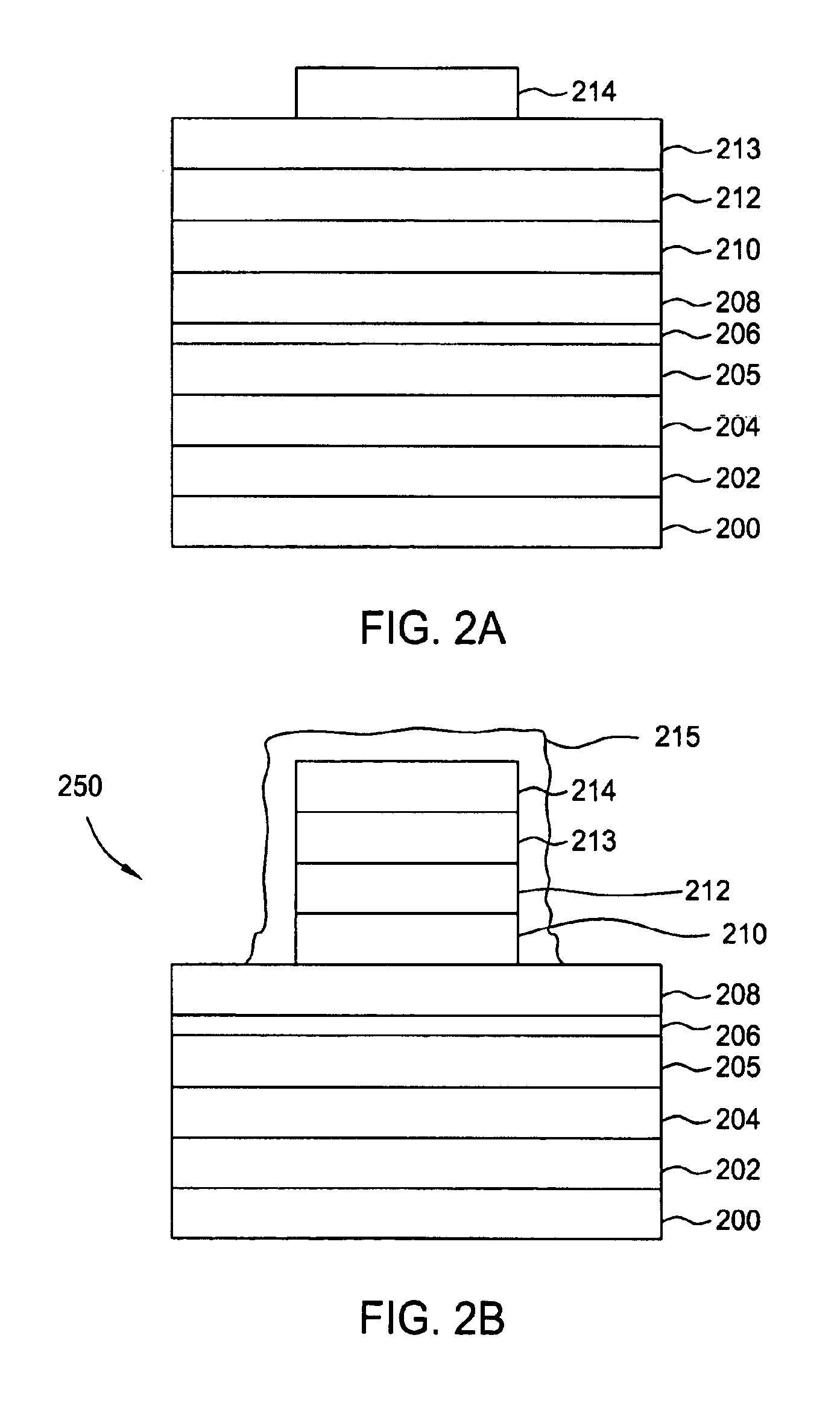
[0016]The present invention generally provides a method of preventing electrical short circuits along the vertical sidewalls of a multi-layer film stack. FIG. 1 depicts a schematic diagram of an etch chamber 110 that may be used to practice embodiments of the invention described herein. The etch chamber may be, for example, a DPS II etch module of the Centura® metal etch system, commercially available from Applied Materials, Inc. of Santa Clara, Calif. The etch chamber 110 comprises at least one inductive coil antenna 112, positioned exterior to a dielectric ceiling 120. The ceiling 120 may be flat, as shown in FIG. 1, or alternatively, the ceiling 120 may have another shape, such as a dome shape. The antenna 112 is coupled to a radio-frequency (RF) source 118 that is generally capable of producing an RF signal having a tunable frequency of about 2 MHz. The RF source 118 is coupled to the antenna 112 through a matching network 119. Process chamber 110 also includes a substrate suppo...


PUM


Abstract

A method for preventing electrical short circuits in a multi-layer magnetic film stack comprises providing a film stack that includes a layer of magnetic material having an exposed surface. A protective layer is deposited on the exposed surface of the magnetic layer. The protective layer may comprise, for example, a fluorocarbon or a hydrofluorocarbon. The film stack is etched and the protective layer protects the exposed surface from a conductive residue produced while etching the film stack. The method may be used in film stacks to form a magneto-resistive random access memory (MRAM) device.

Description

CROSS-REFERENCE TO RELATED APPLICATIONS[0001]This invention claims benefit of U.S. provisional patent application Ser. No. 60 / 365,954, filed Mar. 19, 2002, which is herein incorporated by reference.BACKGROUND OF THE INVENTION[0002]1. Field of the Invention[0003]Embodiments of the present invention generally relate to a method for processing magnetic film stacks. More specifically, the invention relates to a method of preventing an electrical short circuit while fabricating magneto-resistive random access memory (MRAM) devices.[0004]2. Description of the Related Art[0005]Microelectronic devices are generally fabricated on a semiconductor substrate as integrated circuits wherein various layers of materials must be deposited and patterned to form the device. An example of such a device is a magneto-resistive random access memory (MRAM) device.[0006]An MRAM typically comprises a multi-layer film or “film stack” that may be processed to form an information storage element. The film stack...

Claims


Application Information

Patent Timeline
IPC IPC(8): H01L23/00H01L21/00H01L43/12
CPCH01L43/12H01L23/564H01L21/67069H01L2924/0002H10N50/01H01L2924/00
Inventor NALLAN, PADMAPANI C.KUMARHWANG, JENG H.JIN, GUANGXIANGKERNS, RALPH
Owner APPLIED MATERIALS INC
Why Eureka
Try Eureka