Electron beam proximity exposure apparatus and mask unit therefor

a technology of proximity exposure and exposure apparatus, which is applied in the field of exposure apparatus, can solve the problems of increasing manufacturing costs, no practical use, and many problems in terms of productivity, cost, and stability, and achieve the effect of improving throughput and reducing the frequency of taking

Inactive Publication Date: 2005-05-17
TOKYO SEIMITSU
View PDF7 Cites 5 Cited by
  • Summary
  • Abstract
  • Description
  • Claims
  • Application Information

AI Technical Summary

Benefits of technology

[0016]The present invention has been developed in view of the above-described circumstances, and has as its object the improvement of a throughput by red...

Problems solved by technology

However, much finer circuit patterns involve various kinds of problems such as a rapid increase of manufacturing costs.
New types of exposure apparatus such as an electron beam direct lithography apparatus and an X-ray exposure apparatus have been therefore developed, but there still remain many problems in terms of stability, productivity, cost, etc.
However, it was thought that it was of no practical use since it was difficult to eliminate the proximity effect peculiar to the electron beam.
Accordingly, it arises not only a problem of lowered the throughput but also a problem to allow dust and the like to easily adhere, thereby lowering the yield.
Therefore, dust or the like adhering to the surface of the mask causes a serious problem in the above-described electron beam proximity exposure apparatus.
However, since the mask is required to be taken out of the electron beam proximity exposure apparatus once for cleaning and to be then mounted again to the ele...

Method used


Image

  • Electron beam proximity exposure apparatus and mask unit therefor
  • Electron beam proximity exposure apparatus and mask unit therefor
  • Electron beam proximity exposure apparatus and mask unit therefor

Examples


Embodiment Construction

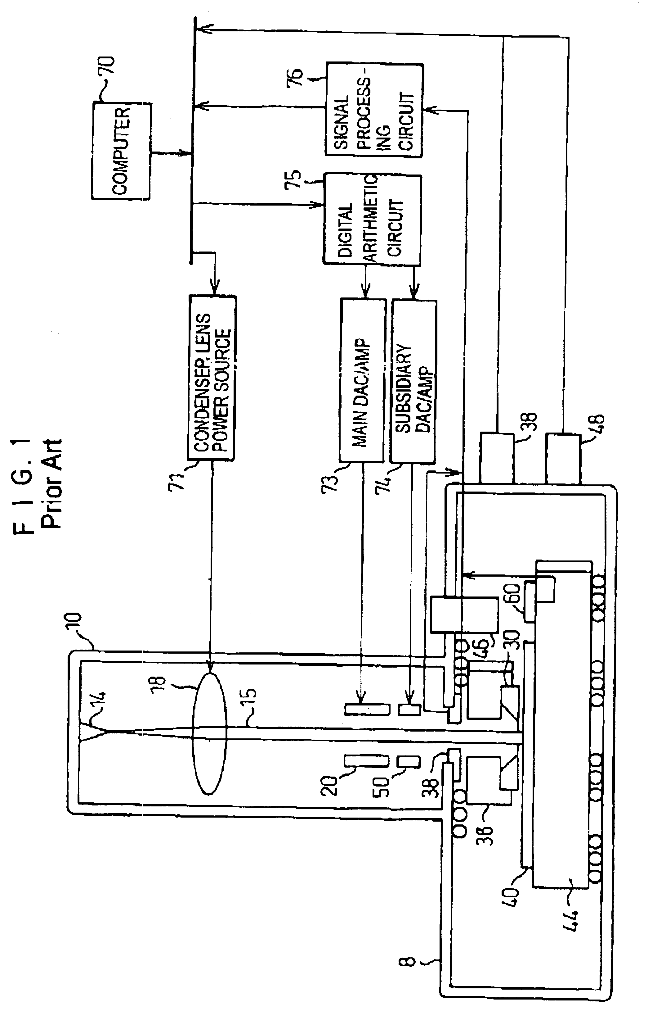
[0029]An electron beam exposure apparatus according to an embodiment of the present invention has a structure similar to that shown in FIG. 1, although contains different points such that the apparatus comprises a mask unit having a plurality of masks instead of a mask 30, and a mask stage 36 has a bigger moving range so that each of the plurality of masks can be positioned on the path of the electron beam.

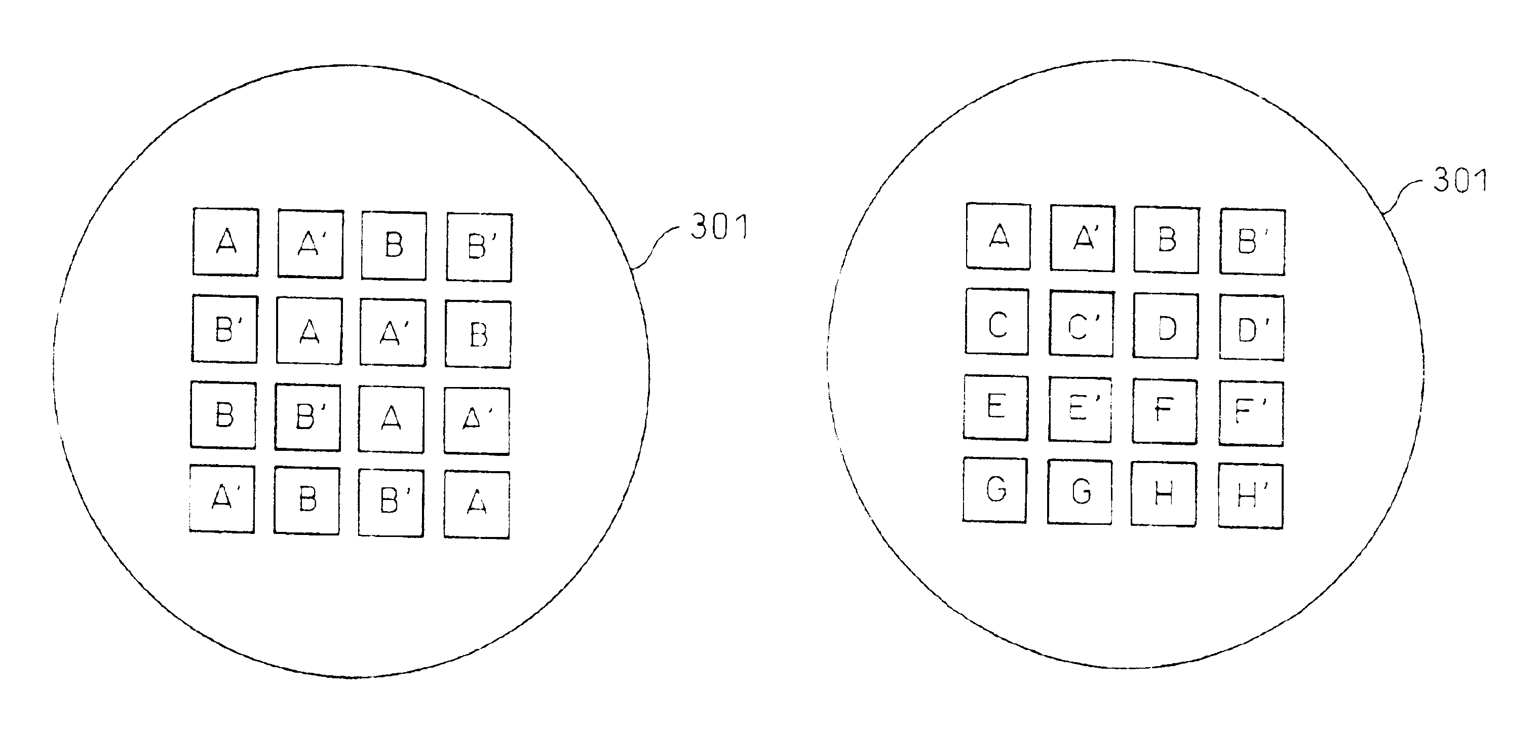
[0030]FIGS. 4(A) and 4(B) are a plan view and a sectional view, respectively, of the mask unit according to an embodiment of the present invention.

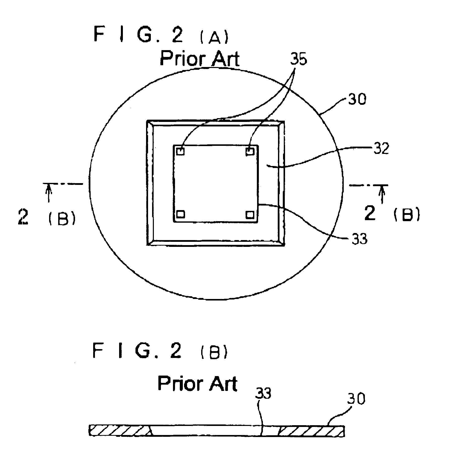
[0031]As shown in FIG. 4(A), a mask unit 301 has sixteen masks 302. Each mask 302 has a shape similar to a portion denoted with the reference number 32 in FIG. 2, in which it is processed in the thickness of a few micrometers or submicrometers and an aperture pattern and a positioning mark are formed within. The masks 302 are formed with some distances away from each other.

[0032]As shown in FIG. 4(B), a portion of each mask 302 is proce...


PUM


Abstract

In an electron beam proximity exposure apparatus comprising an electron beam source, which emits a collimated electron beam, a mask substrate on which a plurality of masks with apertures are formed, a mask moving mechanism, which moves the mask substrate, and a stage, which holds and moves an object, the mask moving mechanism moves the mask substrate so that one of the plurality of masks is arranged on a path of the electron beam in proximity to a surface of the object, and a pattern corresponding to the aperture of the one of the plurality of masks is exposed on the surface of the object with the electron beam having passed through the aperture. Thus, the frequency of taking the mask out of the apparatus to exchange the mask is reduced, so that the throughput of the apparatus is improved.

Description

BACKGROUND OF THE INVENTION[0001]1. Field of the Invention[0002]The present invention relates to an exposure apparatus, which is used to expose fine patterns in a manufacturing process of semiconductor integrated circuits, etc., and a mask unit used therefor, and more particularly to an electron beam proximity exposure apparatus, in which a mask having apertures corresponding to a pattern to be exposed is disposed in proximity to a surface of an object such as a semiconductor wafer, the mask is irradiated with an electron beam, and exposure of the pattern with the electron beam having passed through the apertures is thereby performed, and a mask unit used therefor.[0003]2. Description of the Related Art[0004]Attempts are being made to enhance integration degrees of semiconductor integrated circuits and finer circuit patterns are desired. Presently, a limit of the finer circuit patterns is defined mainly by exposure apparatuses, and a stepper, which is an optical exposure apparatus, ...

Claims


Application Information

Patent Timeline
IPC IPC(8): H01J37/317G21K5/04G03F1/16G03F7/20H01J37/305H01L21/027
CPCB82Y10/00B82Y40/00H01J37/3174H01J2237/31788H01J2237/0458
Inventor SHIMAZU, NOBUOUTSUMI, TAKAO
Owner TOKYO SEIMITSU
Why Eureka
Try Eureka