

Output buffer circuit and integrated semiconductor circuit device with such output buffer circuit
a technology of output buffer circuit and integrated semiconductor circuit, which is applied in the direction of logic circuit coupling/interface arrangement, pulse technique, instruments, etc., can solve the problems of system failure to properly determine the logic level of “1” or “0” and other problems, such as system malfunction, variation in cross-point cp and slew rate cannot be compensated
- Summary
- Abstract
- Description
- Claims
- Application Information
AI Technical Summary
Benefits of technology
Problems solved by technology
Method used
Image


Examples
1st embodiment
[0046]An output buffer circuit according to a first embodiment of the present invention will be described below with reference to the drawings.
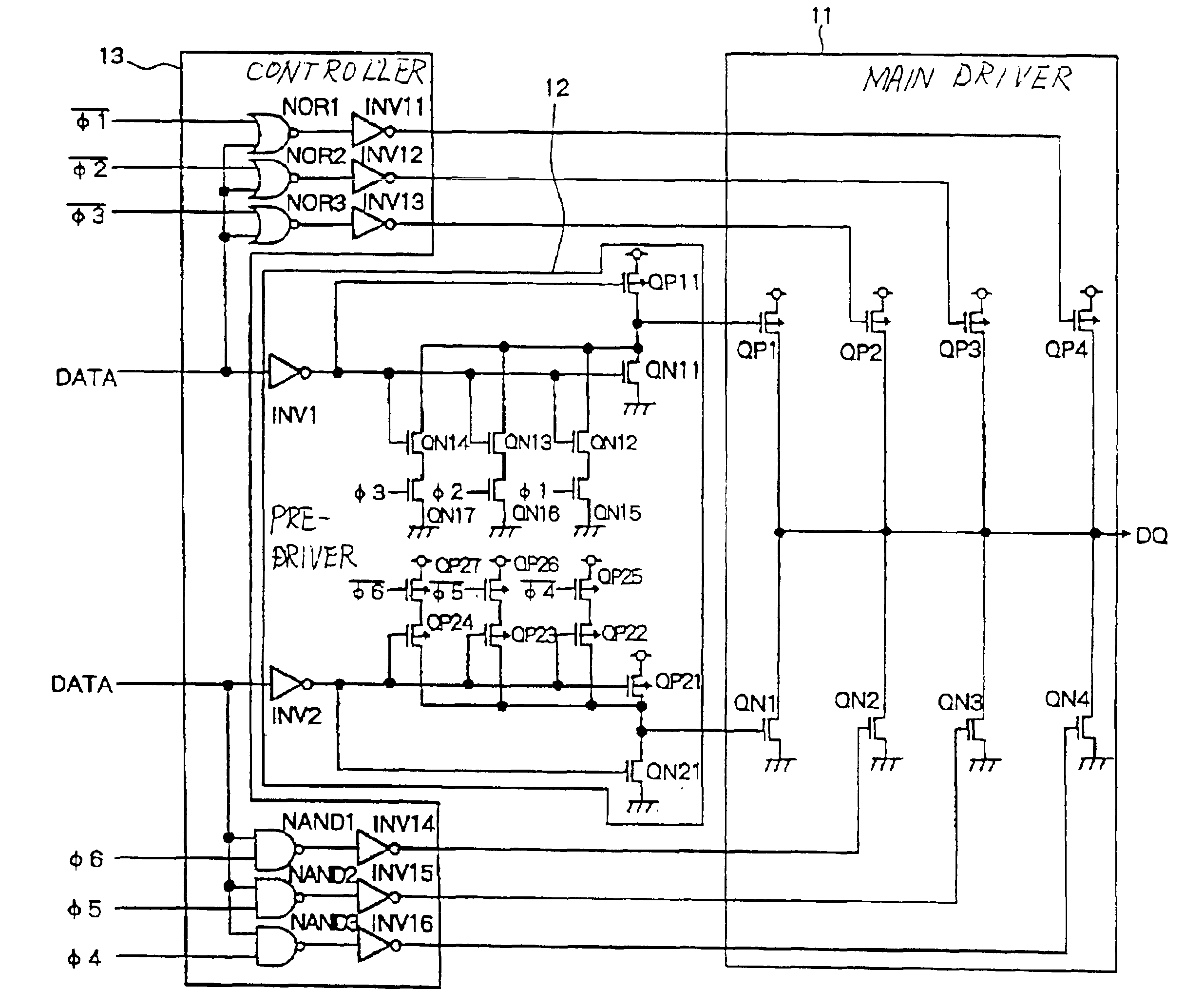
[0047]As shown in FIG. 3, the output buffer circuit according to the first embodiment has main driver 11 for driving a load connected to DQ terminal, main driver 11 having an output impedance which can be changed, a predriver 12 for driving main driver 11 according to data (DATA) read from a sense amplifier and changing the ratio tr / tf of output pulses of main driver 11, and a controller 13 for generating signals to change the output impedance of main driver 11 and the ratio tr / tf of output pulses according to control signals φ1 through φ6 from a control circuit, etc. Control signals / φ1 through / φ6 shown in FIG. 3 are inversions of signals φ1 through φ6. Inverters for inverting signals φ1 through φ6 are omitted from the illustration in FIG. 3.
[0048]For example, control signals φ1 through φ6 are generated from a control circuit 6 according to...
3rd embodiment
[0077]According to a third embodiment, the arrangements of the output buffer circuits according to the first and second embodiments are applied to another circuit.
[0078]As described above, an integrated semiconductor circuit device such as a DDR-SDRAM or the like which operates at a high speed incorporates phase synchronizing circuit 9 for synchronizing data output from output buffer circuit 8 with system clock signal CLK, as shown in FIG. 9.
[0079]Phase synchronizing circuit 9 comprises a DLL as shown in FIG. 9, for example. Phase synchronizing circuit 9 has input buffer circuit 21 for being supplied with system clock signal CLK, variable delay circuit 22 for delaying clock signal CLK1 output from input buffer circuit 21 to generate compensating clock signal CLKOE for compensating for output data timing of output buffer circuit 8, delay monitor circuit 23 for being supplied with compensating clock signal CLKOE and monitoring a delay of output buffer circuit 8, input buffer replica c...
PUM
 Abstract
Description
Claims
Application Information