Flanged terminal pins for DC/DC converters

a technology of dc/dc converters and terminal pins, which is applied in the direction of electrical apparatus construction details, fixed connections, coupling device connections, etc., can solve the problems of affecting the cooling air flow of the dc/dc converter, and affecting the cooling air flow of the open frame converter. , to achieve the effect of minimal interference with the cooling airflow underneath the dc/dc converter

Inactive Publication Date: 2005-05-24
SYNQOR
View PDF29 Cites 29 Cited by
  • Summary
  • Abstract
  • Description
  • Claims
  • Application Information

AI Technical Summary

Benefits of technology

[0015]To address the problems mentioned above, a new through-hole terminal pin is used for mounting dc / dc converters or other circuit modules. In one embodiment, this pin is similar to a standard through-hole pin, but it has a circular flange near its bottom end. The diameter of the flange is greater than the diameter of the PCB hole through which the lower portion of the pin is inserted. The bottom of the flange therefore rests against the PCB's surface. It is located a specified distance from the dc / dc converter's substrate so that it provides the function of a stand-off, but without taking up space on the substrate or requiring a separate part. In addition, its interference with the cooling airflow underneath the dc / dc converter is minimal.
[0016]In another embodiment, the through-hole pin has a flange near or at the top end of the pin where it makes contact with the dc / dc converter's substrate. The top of this flange rests against the bottom of the substrate. This arrangement improves the mechanical connection of the pin to the dc / dc converter's substrate, and it provides one way to ensure the proper z-axis placement of the pin relative to the substrate.
[0018]In a fourth embodiment, the end of the pin has a cross-sectional shape that is pointed along its periphery. This pointed shape facilitates press fitting, or swaging, the pin into a hole of either the substrate, the PCB, or both. The press fit holds the pin in place for later soldering in a hand, wave, or reflow process, and it improves the mechanical strength between the pin and the substrate or PCB.
[0023]Finally, the PCB is passed through a reflow oven in which the solder paste first melts and then solidifies. During this step, the solder paste between each pin flange and the PCB wicks down into the corresponding PCB hole. The final solder joint between the pin and the PCB will therefore exist both underneath the flange and inside the PCB hole. With a properly designed pad and screening process, there will also be a fillet of solder around the outer edge of the flange to provide additional mechanical stress relief. The result is a very strong mechanical connection between the pin and the PCB, as well as a low resistance electrical connection between the pin and both the inner and outer conductive layers of the PCB.
[0024]The flange facilitates this special soldering process. It provides a region in which the solder paste directly contacts both the pin and the PCB. As the solder melts, it readily wicks along the surface of the flange and down the pin such that it fills the gap between the pin and the PCB hole's via metalization.
[0026]In this alternative reflow soldering process the end of the inserted pin should not extend beyond the bottom of the PCB. Otherwise, it might interfere with the solder application step. In fact, it is useful for the end of the inserted pin not to reach the bottom side of the PCB (i.e., for the end to be inside the PCB). Such an alignment gives a small “well” in the hole area, which increases the amount of solder that can be applied in this area. A flange near the bottom end of the pin facilitates the correct insertion depth of the pin into the PCB hole, although there are other well-known means for controlling this depth.

Problems solved by technology

Because these standoffs either abut or are attached to the converter's substrate, they take up space on the substrate that could otherwise be used for electronic components.
They also partially or totally block the cooling air from flowing under the open frame converter.
Finally, the standoff represents an additional cost for the part and for its attachment to the converter.
As the distance between the leads on SMT packages gets smaller, it becomes more difficult to pass these packages through a wave solder process and not have solder bridges form between adjacent leads.
Furthermore, the heating associated with the wave soldering process compromises the quality of the SMT components and their attachments to the PCB.
One important problem with all of these approaches for making a surface mountable dc / dc converter is the relative weakness of a surface mount joint compared to a through-hole pin.
This problem is particularly important since dc / dc converters have a higher mass than most components, and the mounting joints are therefore more susceptible to shock and vibration stresses.
Another problem with a surface mountable dc / dc converter is that the converter's pins make electrical contact with only the outer conductive layer in the PCB.

Method used


Image

  • Flanged terminal pins for DC/DC converters
  • Flanged terminal pins for DC/DC converters
  • Flanged terminal pins for DC/DC converters

Examples


Embodiment Construction

[0056]A description of preferred embodiments of the invention follows.

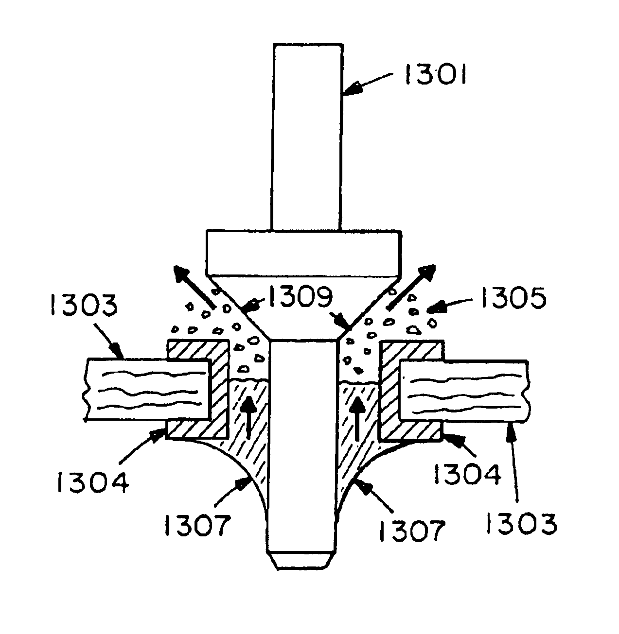
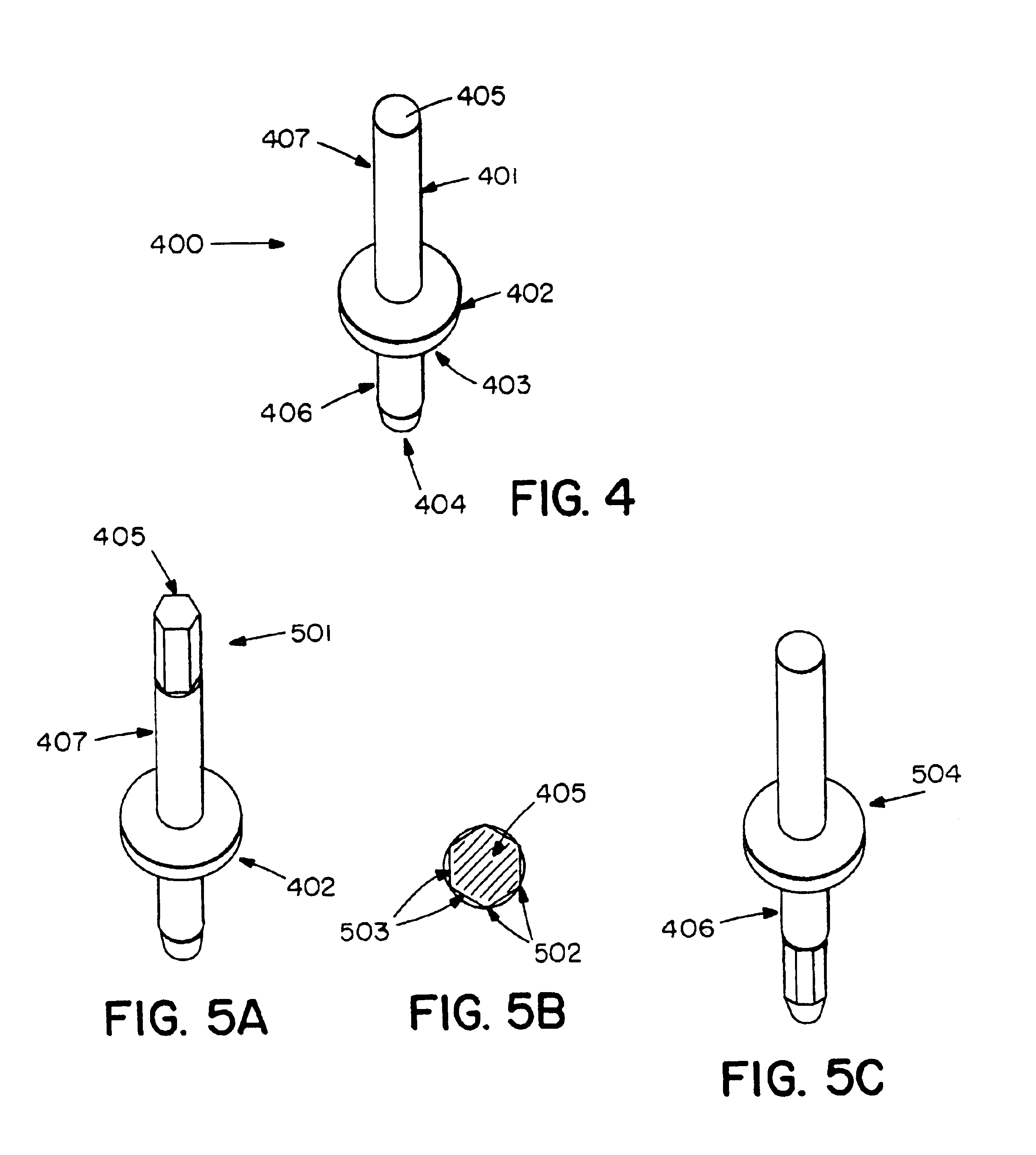
[0057]Throughout this discussion and in the figures we will assume the cross-section of the pin and its flange is circular. One skilled in the art would know how to incorporate the concepts presented here for other cross-sectional shapes, such as triangular or rectangular.

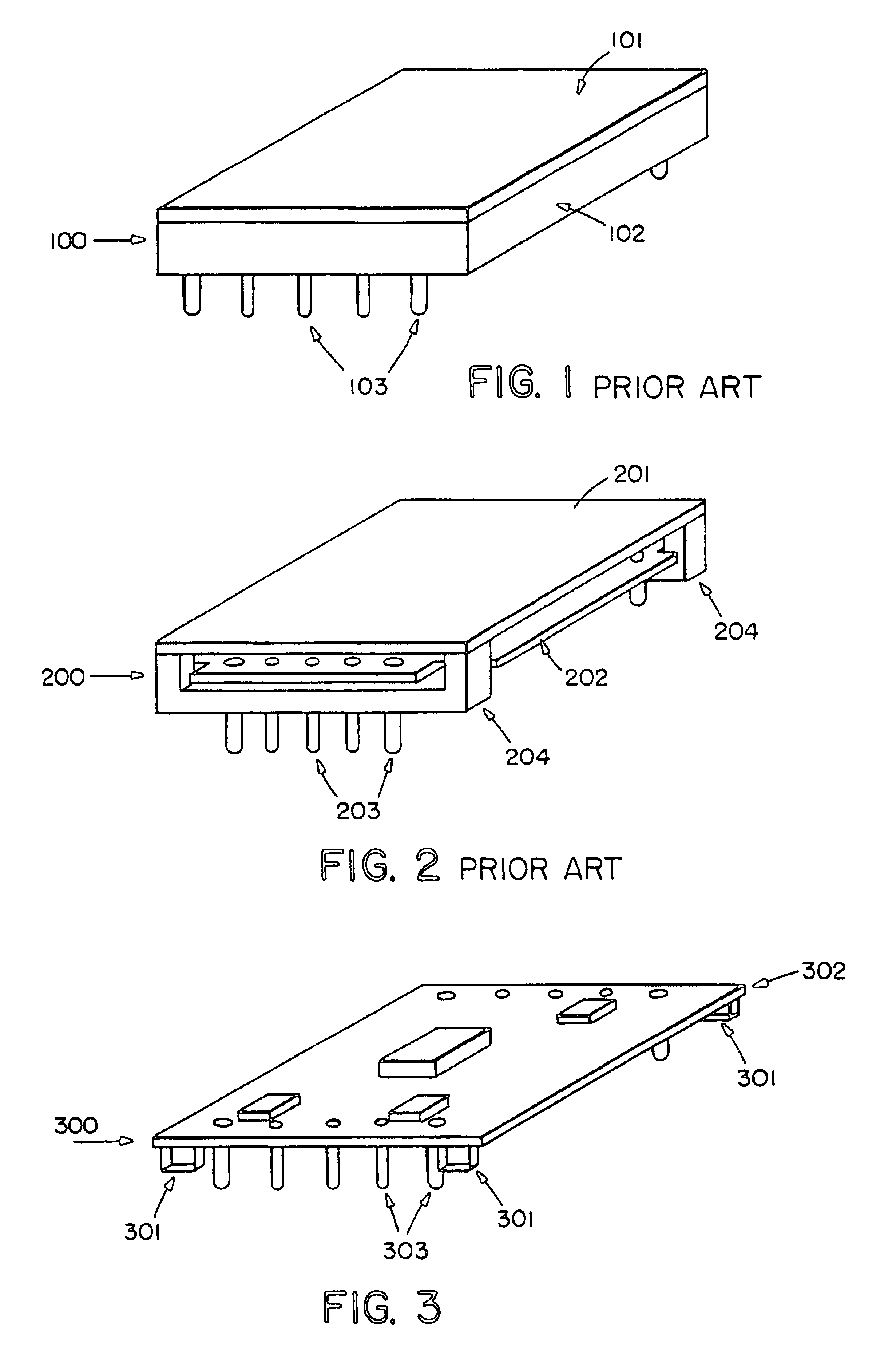
[0058]FIG. 1 shows a typical dc / dc converter 100 with a metal baseplate 101 (to which a heatsink might be attached), a housing or potting 102 (inside which is the converter's circuitry), and its through-hole pins 103. The pins have various diameters (e.g. 40, 60, and 80 mils) to handle their rated current, and various lengths below the housing (e.g. 110, 145, and 180 mils) to pass all the way through the PCB holes.

[0059]FIG. 2 shows an open-frame dc / dc converter 200 with a metal baseplate 201 and through-hole pins 203. Since there is no housing or potting in this converter, the converter's circuitry 202 is visible. In some open-frame converters, ...


PUM

PropertyMeasurementUnit
dc voltageaaaaaaaaaa
voltageaaaaaaaaaa
melting temperatureaaaaaaaaaa

Abstract

A dc / dc converter is mounted to a printed circuit board with rigid terminal pins which extend into a converter substrate to provide electrical connection to circuitry on the substrate. A terminal pin includes a flange which abuts the printed circuit board and spaces the converter substrate from the printed circuit board. Connection to the printed circuit board is made by solder provided between the flange and the circuit board.

Description

RELATED APPLICATIONS[0001]This application is a Continuation-in-Part of application Ser. No. 10 / 378,549, filed on Mar. 3, 2003. The entire teachings of the above applications are incorporated herein by reference.BACKGROUND OF THE INVENTION[0002]Designers are increasingly using distributed power supply architectures for large electronic equipment. With this type of architecture, electrical power is bussed throughout the equipment at a relatively high dc voltage, such as 48 volts. dc / dc converters mounted near the load (and often on the same printed circuit board as the load) then step this high voltage down to the low voltage required by the load (e.g. 3.3V), typically through an isolating transformer.[0003]These point-of-load dc / dc converters typically have a low height (e.g. 0.5″) so that the designer can place adjacent load boards close together in a card rack. The plan-view size of the converter must also be as small as possible to leave more room on the load board for the load c...

Claims


Application Information

Patent Timeline
Patent Type & Authority Patents(United States)
IPC IPC(8): H05K3/36H05K3/34H05K7/14H05K1/14H05K3/30H01R12/55H05K3/32
CPCH01R9/091H05K3/3447H05K7/142H05K3/368H05K1/141H05K3/308H05K3/3484Y10T29/49165H05K2201/1081H05K2201/10871H05K2203/0545H01R12/58H05K3/3485
Inventor PITZELE, LENNART
Owner SYNQOR
Why Eureka
Try Eureka