Methods of manufacturing electron-emitting device, electron source, and image display apparatus

a technology of electron emitting device and image display device, which is applied in the manufacture of electric discharge tube/lamp, tube/lamp factory adjustment, and screen, etc., can solve the problems of complex management of respective steps and the manufacture of an image-forming apparatus that uses a conventional method, so as to save power consumption of the apparatus, improve the electron-emitting characteristics, and improve the effect of electron-emitting characteristics

Inactive Publication Date: 2005-05-24
CANON KK
View PDF42 Cites 35 Cited by
  • Summary
  • Abstract
  • Description
  • Claims
  • Application Information

AI Technical Summary

Benefits of technology

[0018]Further, in the case where the electron-emitting device is used for an image-forming apparatus such as a display, further improvement in electron-emitting characteristics is desired in order to save power consumption of the apparatus.
[0019]Moreover, it is desired that the image-forming apparatus that uses the electron-emitting device is manufactured easier and simpler and at lower cost.
[0025](C) forming a gap in a film obtained by reducing a resistivity of the polymer film,
[0030](C) forming a gap in a film obtained by reducing the resistivity of the polymer film in the vicinity of one of the pair of electrodes, by flowing a current to the film obtained by reducing the resistivity of the polymer film, wherein the film obtained by reducing the resistivity of the polymer film has an activation energy for electrical conduction of 0.3 eV or less.

Problems solved by technology

However, manufacturing of an image-forming apparatus that uses such a conventional electron-emitting device has the following problems.
That is, the manufacturing includes many additional steps such as repeated energization steps in the “energization forming step” and the “activation step” and a step of forming a preferable atmosphere in each step, and thus, management of respective steps has been complicated.

Method used


Image

  • Methods of manufacturing electron-emitting device, electron source, and image display apparatus
  • Methods of manufacturing electron-emitting device, electron source, and image display apparatus
  • Methods of manufacturing electron-emitting device, electron source, and image display apparatus

Examples


embodiment

[0206]The present invention will be hereinafter described more in detail with reference to embodiments.

first embodiment

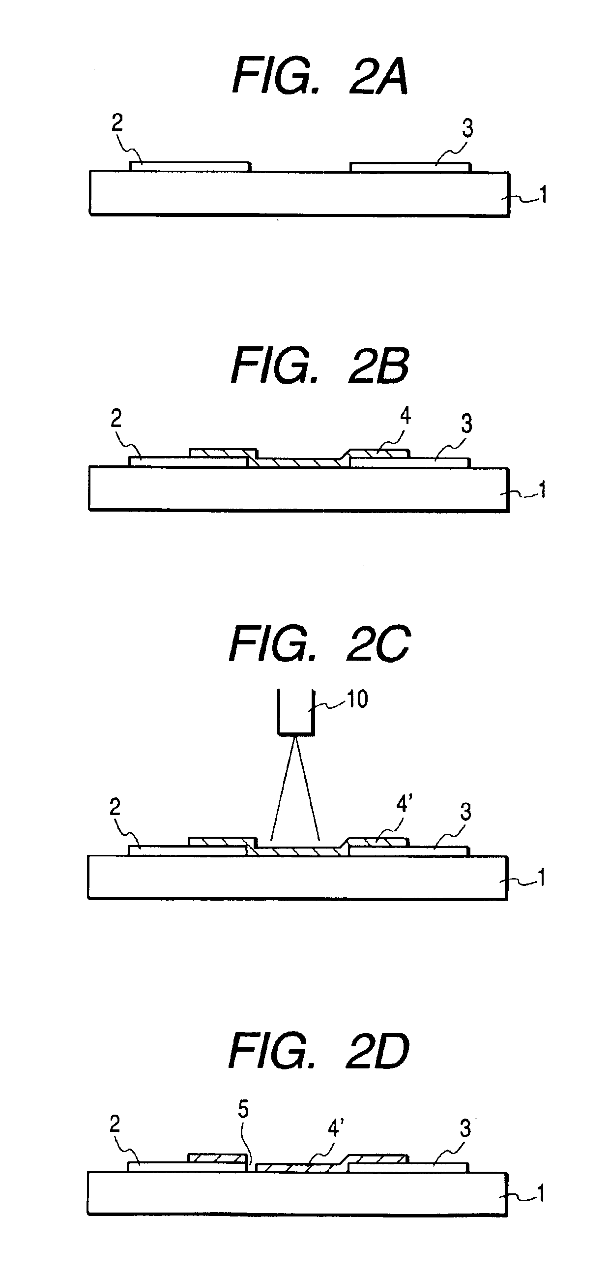
[0207]In this embodiment, the electron-emitting device manufactured by the manufacturing method shown in FIGS. 2A to 2D was used. Details of the manufacturing process will be hereinafter described.

Step 1

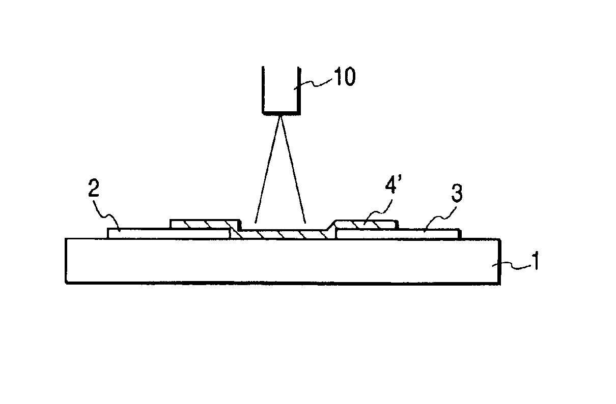
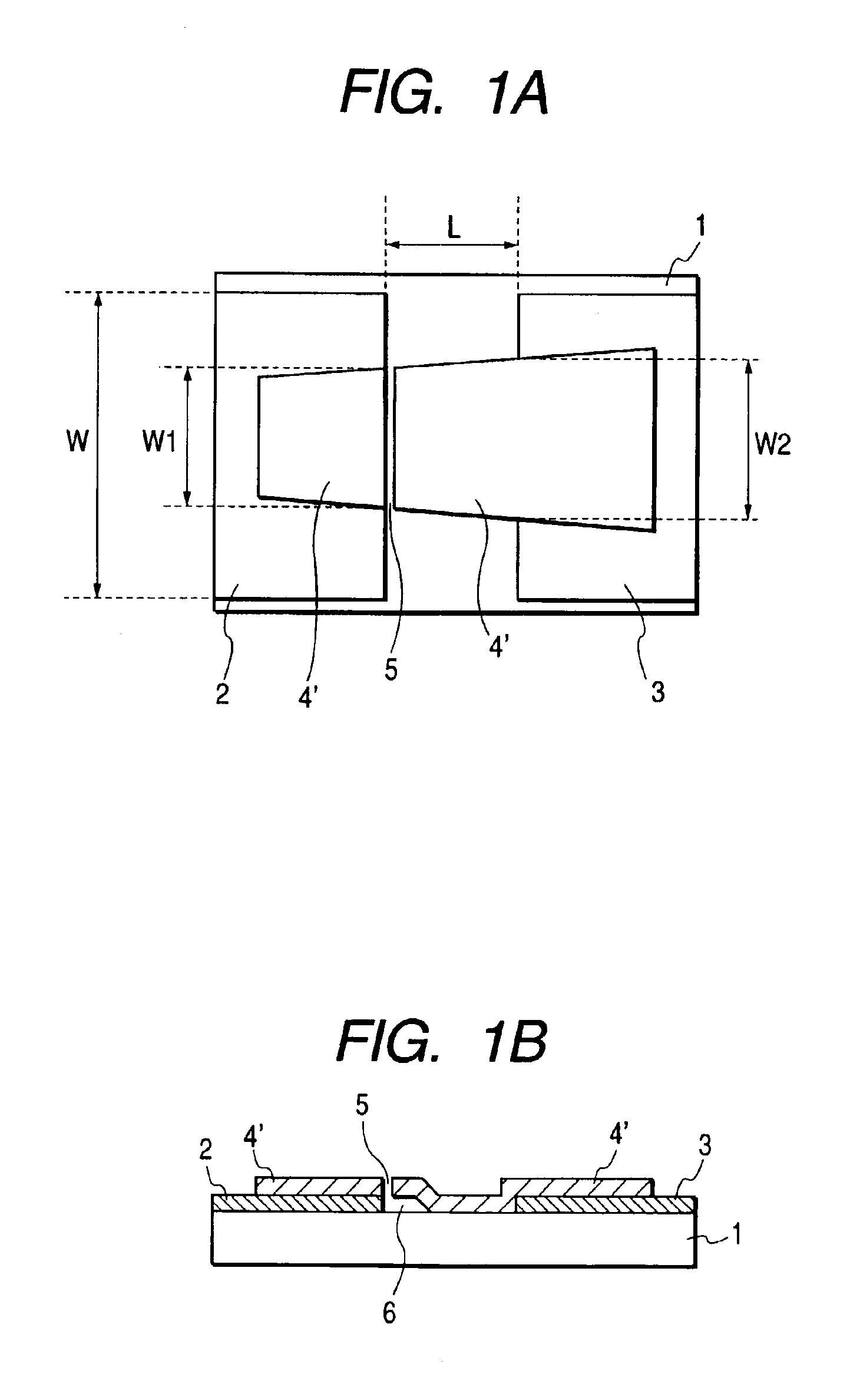
[0208]A Pt film with a thickness of 100 nm was deposited on the glass substrate 1 by the sputtering method, and electrodes 2 and 3 consisting of the Pt film were formed with the photolithography technique (FIG. 2A). Note that a distance between the electrodes 2 and 3 was set to 10 μm. “PD200” manufactured by Asahi Glass Co., Ltd. was used as the substrate 1. Physical property values of this glass are as follows: specific heat: csub=653 J / kg·K, specific gravity: ρsub=2730 kg / m3, and heat conductivity: λSub=0.09 W / m·K. In addition, when an absorption coefficient of a wavelength around 800 nm of this glass was measured, it was approximately 5%. Further, a not-shown wiring for supplying a current is connected to the electrodes 2 and 3, respectively. The wiring is arranged on the substrat...

second embodiment

[0226]In this embodiment, an image-forming apparatus 100 schematically shown in FIG. 16 was manufactured. Reference numeral 102 denotes an electron-emitting device of the present invention. A method of manufacturing the image-forming apparatus of this embodiment will be described with reference to FIGS. 6 to 12, FIG. 16, FIGS. 17A and 17B.

[0227]FIG. 12 schematically shows a part of an electron source, which is constituted by a rear plate 1, a plurality of electron-emitting devices of the present invention formed on the rear plate 1, and wiring for applying a signal to each electron-emitting device, in an enlarged manner. Reference numeral 1 denotes a rear plate; 2 and 3, electrodes; 5′, a gap; 4′, a carbon film; 62, X-directional wiring; 63, Y-directional wiring; and 64, an interlayer insulating layer.

[0228]PD200 of Asahi Glass Co., Ltd. was used as the rear plate 1. Each property value is as follows:[0229]Specific heat: csub=653 J / kg·K[0230]Specific gravity: ρsub=2730 kg / m3 [0231]H...


PUM


Abstract

In a process of reducing a resistivity of a polymer film for carbonization in a surface conduction electron-emitting device, by irradiating an energy beam onto the polymer film, when an energy intensity of the beam given in a unit area in a unit time is assumed to be W W / m2, W satisfies a formula W≧2×T×(ρsub·Csub·λsub / τ)1 / 2, where T is defined as a temperature ° C. at which the polymer film is heated for one hour in a vacuum degree of 1×10⁻⁴ Pa to reduce a resistivity of the polymer film to 0.1 Ω·cm, Csub is a specific heat J / kg·K of the substrate, ρsub is a specific gravity kg / m3 of the substrate, λsub is a heat conductivity W / m·K of the substrate, and τ is an irradiation time in the range of 10−9 sec to 10 sec.

Description

BACKGROUND OF THE INVENTION[0001]1. Field of the Invention[0002]The present invention relates to a method of manufacturing an electron-emitting device, a method of manufacturing an electron source by processing units into a large number of electron-emitting devices, and a method of manufacturing an image-forming apparatus, such as an image display apparatus, which is structured by using the electron source.[0003]2. Related Background Art[0004]Up to now, a surface conduction electron-emitting device has been known as an electron-emitting device.[0005]A structure, a manufacturing method, and the like of the surface conduction electron-emitting device are disclosed, for example, in Japanese Patent Laid-open Gazette No. 8-321254.[0006]A structure of a typical surface conduction electron-emitting device disclosed in the above-mentioned publication or the like is schematically shown in FIGS. 13A and 13B, which are respectively a plan view and a sectional view of the surface conduction ele...

Claims


Application Information

Patent Timeline
Patent Type & Authority Patents(United States)
IPC IPC(8): H01J9/24H01J9/00H01J9/04H01J9/02H01J1/316H01J31/12
CPCH01J31/127H01J9/027
Inventor MIZUNO, HIRONOBUIWAKI, TAKASHITAKEDA, TOSHIHIKOSUZUKI, NORITAKEMIYAZAKI, KAZUYANUKANOBU, KOKI
Owner CANON KK
Why Eureka
Try Eureka