

Encapsulated semiconductor package free of chip carrier
- Summary
- Abstract
- Description
- Claims
- Application Information
AI Technical Summary
Benefits of technology
Problems solved by technology
Method used
Image

Examples
Embodiment Construction
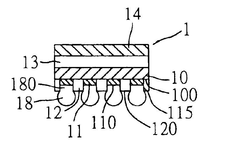
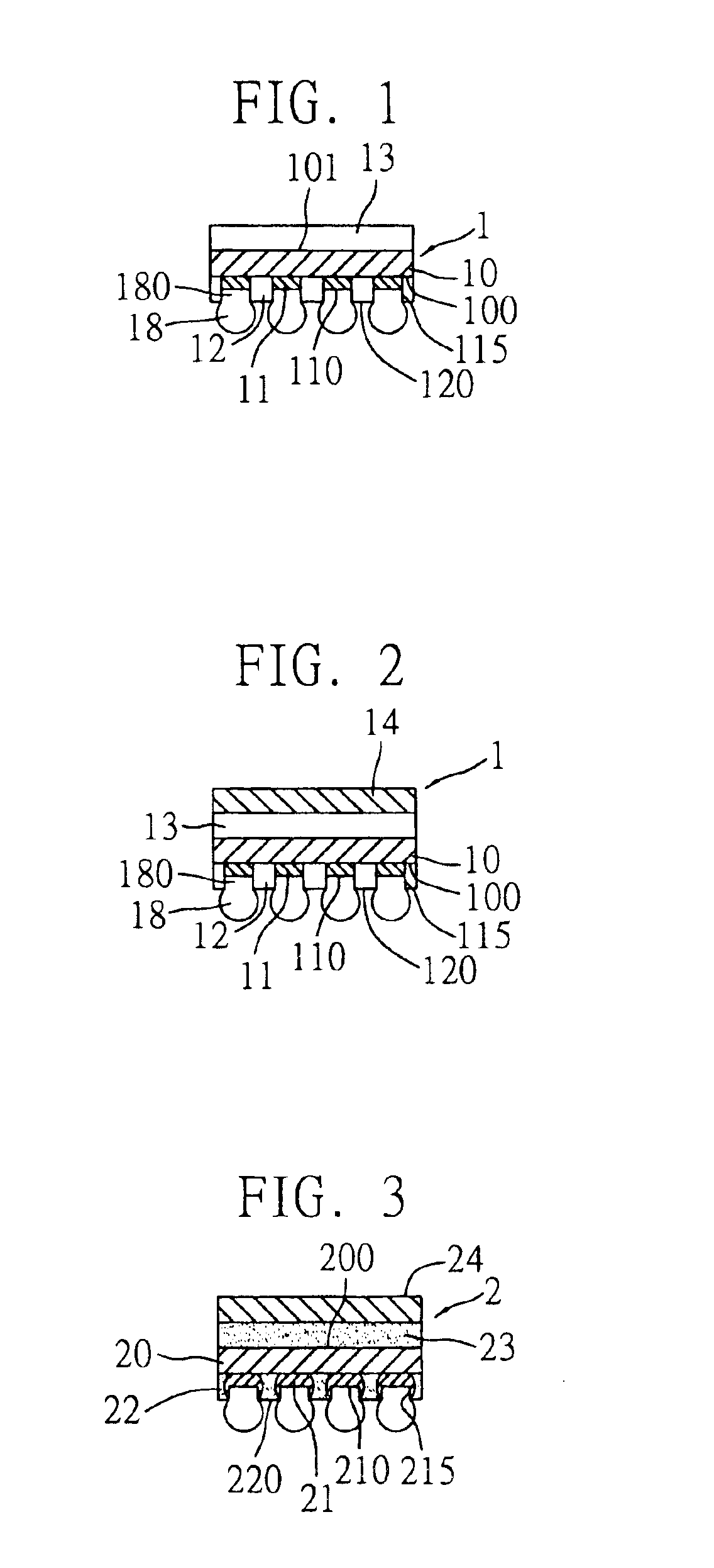
[0016]FIG. 1 illustrates a semiconductor package 1 according to a first embodiment of the present invention. As shown FIG. 1, the semiconductor package 1 is provided with a chip 10 having an active surface 100 and a non-active surface 101 opposed to the active surface 100, wherein a plurality of contacts (not shown) are formed on the active surface 100, for allowing a plurality of connecting bumps 11 made of conductive metal to be implanted at corresponding contacts by conventional printing technique. Each of the contacts on the active surface 100 can be a bond pad, or a connecting pad that is formed by redistributing a corresponding bond pad and electrically connected to the redistributed bond pad by conductive traces. Thereby, the chip 10 would be electrically coupled to the connecting bumps 11 that are bonded to the active surface 100 of the chip 10. Since forming of bond pads or connecting pads employs conventional technology, it is not to be further described herein.
[0017]Moreo...
PUM
| Property | Measurement | Unit |
|---|---|---|
| Mechanical strength | aaaaa | aaaaa |
| Electrical conductor | aaaaa | aaaaa |
Abstract
Description
Claims
Application Information