Self-oriented bundles of carbon nanotubes and method of making same

a carbon nanotube and self-oriented technology, applied in the manufacture of electrode systems, electric discharge tubes/lamps, metal/metal-oxide/metal-hydroxide catalysts, etc., can solve the problems of difficult bulk work, impossibly tangled mess resembling a hairball, and the lik

Inactive Publication Date: 2005-05-31
THE BOARD OF TRUSTEES OF THE LELAND STANFORD JUNIOR UNIV
View PDF15 Cites 104 Cited by
  • Summary
  • Abstract
  • Description
  • Claims
  • Application Information

AI Technical Summary

Benefits of technology

[0027]The above summary of the present invention is not intended to describe each illustrated embodiment or every implementat

Problems solved by technology

However, it has been unclear how to realize a field emission device exploiting carbon nanotubes.
They are difficult to work with in bulk, and, on a microscopic level, often form an impossibly tangled mess resembling a hairball.
A problem with present methods of making carbon nanotube field emitters is that it is not clear how to pattern the carbon nanotube to provide arrays of emitters.
S

Method used


Image

  • Self-oriented bundles of carbon nanotubes and method of making same
  • Self-oriented bundles of carbon nanotubes and method of making same
  • Self-oriented bundles of carbon nanotubes and method of making same

Examples


Embodiment Construction

[0035]The present invention is believed to be applicable to a variety of different types of devices, and the invention has been found to be particularly suited for field emission devices and other devices employing carbon nanotubes. While the present invention is not necessarily limited to such applications, various aspects of the invention may be appreciated through a discussion of various examples using this context.

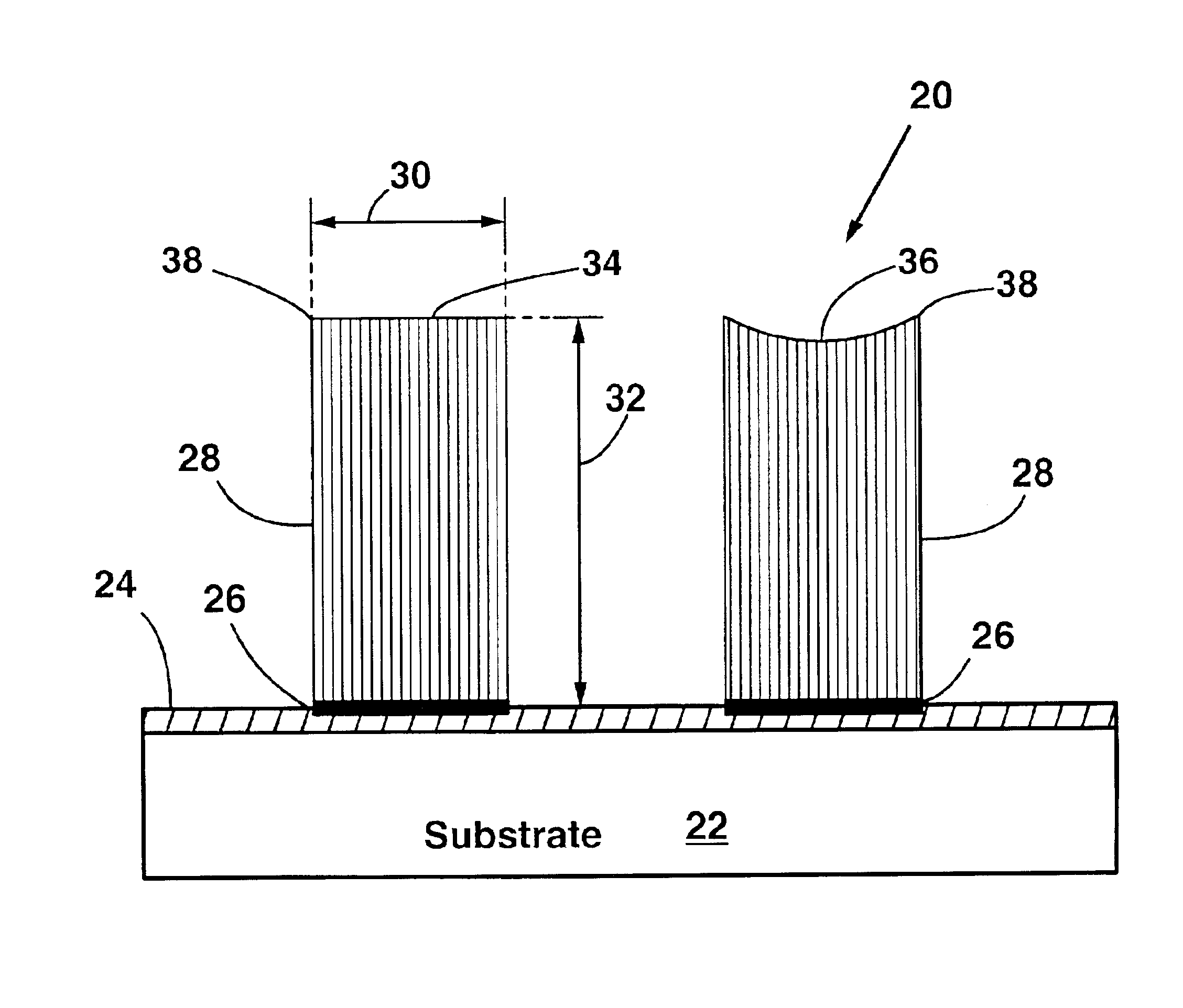
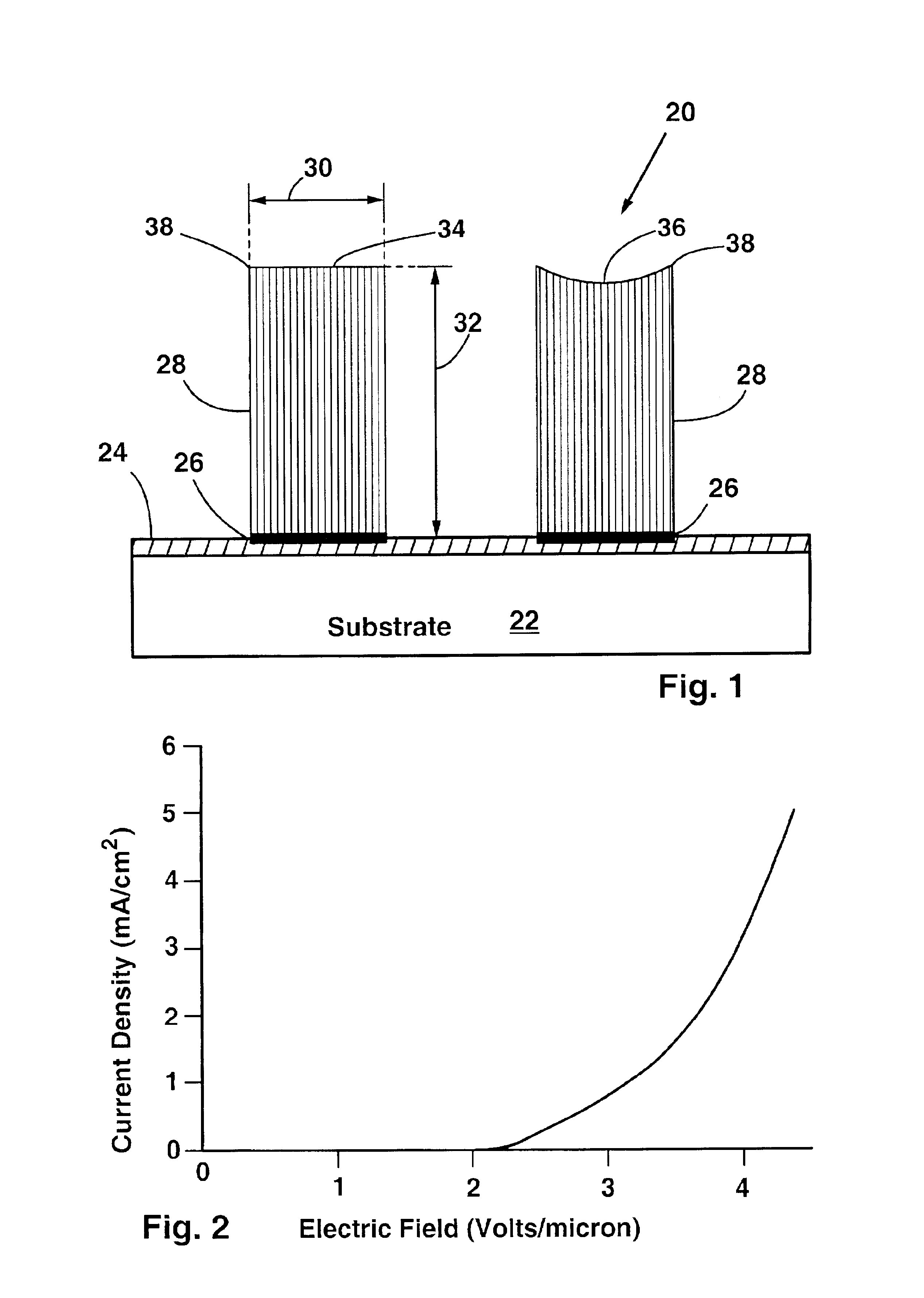
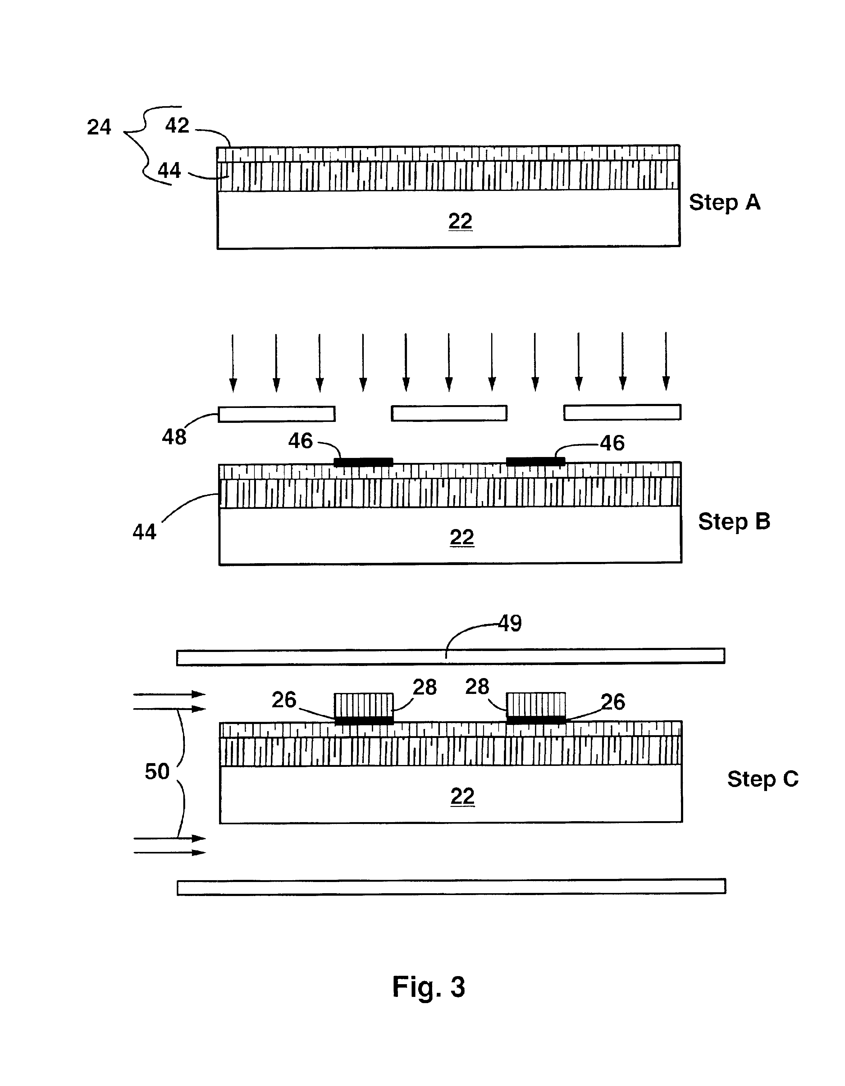
[0036]FIG. 1 shows a field emission device 20 according to an example embodiment of the present invention. The device has a substrate 22 with a porous top layer 24. The substrate 22 and top layer 24 are made of silicon, although other substrate materials can also be used. Disposed on the porous top layer 24 are patterns of catalyst material 26. In one instance, the catalyst material 26 is a thin film of iron oxide. Extending from the catalyst material patterns 26 are carbon nanotube bundles 28, which are perpendicular to the substrate 22. The carbon nanotubes comprisin...


PUM

PropertyMeasurementUnit
Diameteraaaaaaaaaa
Temperatureaaaaaaaaaa

Abstract

A field emission device having bundles of aligned parallel carbon nanotubes on a substrate. The carbon nanotubes are oriented perpendicular to the substrate. The carbon nanotube bundles may be up to 300 microns tall, for example. The bundles of carbon nanotubes extend only from regions of the substrate patterned with a catalyst material. Preferably, the catalyst material is iron oxide. The substrate is preferably porous silicon, as this produces the highest quality, most well-aligned nanotubes. Smooth, nonporous silicon or quartz can also be used as the substrate. The method of the invention starts with forming a porous layer on a silicon substrate by electrochemical etching. Then, a thin layer of iron is deposited on the porous layer in patterned regions. The iron is then oxidized into iron oxide, and then the substrate is exposed to ethylene gas at elevated temperature. The iron oxide catalyzes the formation of bundles of aligned parallel carbon nanotubes which grow perpendicular to the substrate surface. The height of the nanotube bundles above the substrate is determined by the duration of the catalysis step. The nanotube bundles only grow from the patterned regions.

Description

CROSS-REFERENCE TO RELATED APPLICATIONS[0001]This application is a continuation of patent application 09 / 191,728, now U.S. Pat. No. 6,232,706, filed Nov. 12, 1998, which is herein incorporated by reference, to which priority is claimed under 35 U.S.C. §120.FIELD OF THE INVENTION[0002]This invention relates generally to carbon nanotubes. The present invention also relates to methods for making bundles of aligned carbon nanotubes. The present invention is also related to carbon nanotube field emission devices such as used in flat panel displays.BACKGROUND[0003]Field emission devices have potential applications in flat panel displays. Field emitters used in flat panel displays must be stable, long lasting and should have a relatively uniform emission over the surface of the display.[0004]Carbon nanotubes are very small tube-shaped molecules having the structure of a graphite molecule rolled into a tube. Carbon nanotubes are electrically conductive along their length, chemically stable,...

Claims


Application Information

Patent Timeline
IPC IPC(8): C01B31/00C01B31/02H01J9/02B01J23/745B01J37/02B01J37/14C23C14/04C23C14/14C23C16/26H01J1/304H01J29/04
CPCB82Y10/00B82Y30/00B82Y40/00C01B31/0233H01J1/304H01J9/025Y10S977/939C01B2202/08H01J2201/30469C01B2202/06C01B32/162
Inventor DAI, HONGJIEFAN, SHOUSHANCHAPLINE, MICHAELFRANKLIN, NATHANTOMBLER, THOMAS
Owner THE BOARD OF TRUSTEES OF THE LELAND STANFORD JUNIOR UNIV
Why Eureka
Try Eureka