Optical module capable of improving coupling efficiency and suppressing fluctuation of coupling loss and its manufacturing method
Active Publication Date: 2005-05-31
NEC CORP
View PDF22 Cites 64 Cited by
Summary
Abstract
Description
Claims
Application Information
AI Technical Summary
This helps you quickly interpret patents by identifying the three key elements:
Problems solved by technology
Method used
Benefits of technology
Benefits of technology
[0011]It is an object of the present invention to provide an optical module capable of improving the coupling efficiency and suppressing the fluctuation of the coupling loss.
Problems solved by technology
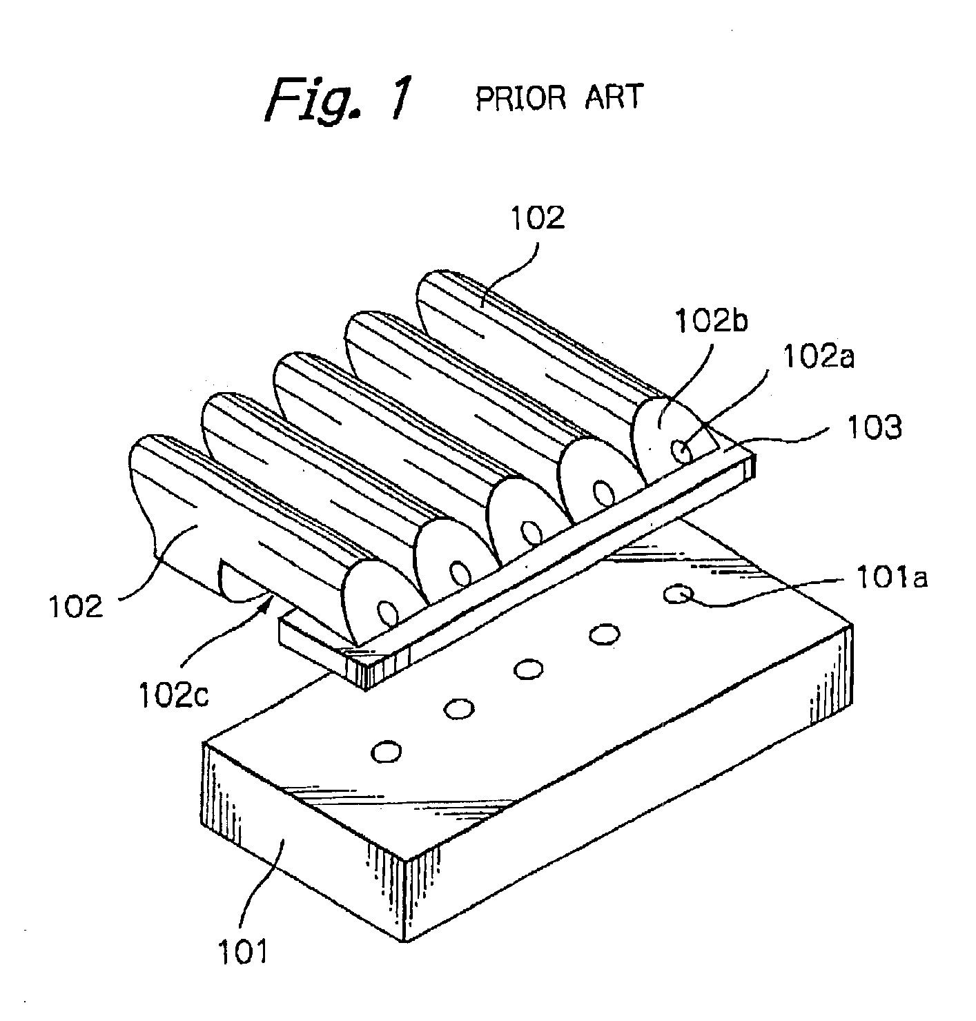
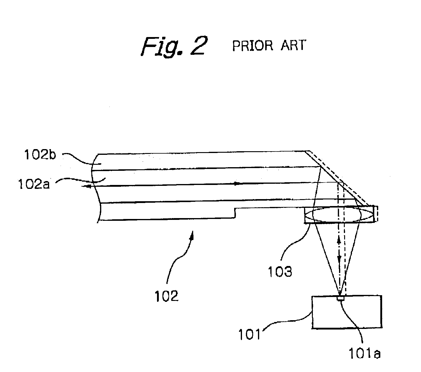
In the above-described first prior art optical module, however, if the alignment of the optical fibers to the LSI package fluctuates, the coupling efficiency therebetween deteriorates.
In the above-described second prior art optical module, however, since the mirror and the half mirror are protruded from the bottom surface of the optical fiber, the coupling between the optical fiber and the package is carried out by a transparent adhesive layer, so that it is impossible to remove the optical fiber from the package.
If the optical fiber is forcibly removed from the package and is again fixed to the package or another package, the coupling loss fluctuates.
Method used
Image
Click on the blue label to locate the original text in one second.
Reading with bidirectional positioning of images and text.
Examples
first embodiment
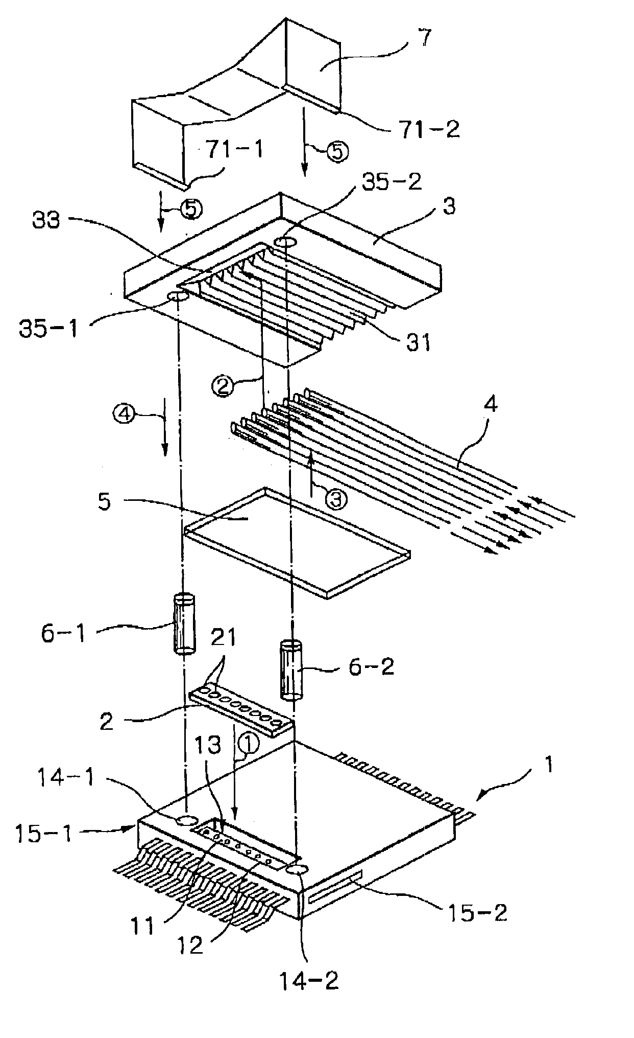
[0035]In FIG. 4, which illustrates the optical module according to the present invention, an LSI package 1 includes LSI chips (not shown), and surface-emitting laser diodes 11 and surface-receiving PIN photodiodes 12 electrically connected to the LSI chips. For example, the pitch of the laser diodes 11 and the pitch of the PIN photodiodes 12 are 250 μm. The laser diodes 11 and the PIN photodiodes 12 are exposed by a rectangular opening 13 on the upper side of the LSI package 1. Also, guide recesses 14-1 and 14-2 are perforated on the upper side of the LSI package 1. Further, recesses 15-1 and 15-2 are perforated on the sides of the LSI package 1.
[0036]A microlens array plate 2 includes microlenses 21 corresponding to the laser diodes 12 and the PIN photodiodes 13. In this case, the microlens array plate 2 can be fitted into the rectangular opening 13 of the LSI package 1, and the pitch of the microlenses 21 is 250 μm, for example.
[0037]An optical array connector, i.e., a fiber array...
second embodiment
[0055]In FIG. 9, which illustrates the optical nodule according to the present invention, an optical waveguide, array 4′ is provided instead of the optical fibers 4 of FIG. 4, and a recess 31′ is provided instead of the V-shaped grooves 31 of FIG. 4 in an optical array connector 3′. Assembling and disassembling operation of the optical module of FIG. 9 can be carried out in a similar way as in the optical module of FIG. 4. Also, the modifications of FIGS. 7 and 8 can be applied to the optical module of FIG. 9.
third embodiment
[0056]In FIG. 10, which illustrates the optical module according to the present invention, a capillary 31″ is provided instead of the V-shaped grooves 31 of FIG. 4, Assembling and disassembling operation of the optical module of FIG. 10 can be carried out in a similar way as in the optical module of FIG. 4. Also, the modifications of FIGS. 7 and 8 can be applied to the optical module of FIG. 10.
[0057]In the above-described embodiments, the package 1 is manufactured by a transfer molding process using resin, so that the guide holes 14-1 and 14-2 (the balls 14′-1 and 14′-2 the protrusions 14″-1 and 14″-2) and the recesses 15-1 and 15-2 can be simultaneously formed. On the other hand, the fiber array connector 3 (optical array connector 3′) is manufactured by a transfer moldingprocessing resin, so that the V-shaped grooves 31, vertical stopper face 32, the oblique face 33 and the vertical stopper face 33, the guide recesses 35-1 and 35-2 (the recesses 35′-1, 35′-2, 35″-1 and 35″-2) ca...
PUM
Abstract
In an optical module, a package includes an array of first optical elements and at least one first positioning member. A microlens array plate including microlenses is fixed to the package, so that each of the microlenses corresponds to one of the first optical elements. An optical array connector mounts second optical elements thereon. The optical array connector has a light path bending portion for bending light paths of the second optical elements and at least one second positioning member. The optical array connector abuts against the package by aligning the second positioning member to the first positioning member so that each of the first optical elements corresponds to one of the second optical elements, A clamping member clamps the optical, array connector to the package.
Description
BACKGROUND OF THE INVENTION[0001]1. Field of the Invention[0002]The present invention relates to an optical module formed by a package for receiving and emitting light and an optical connector, and more particularly, to the improvement of a coupling structure between the package and the optical connector and its manufacturing method.[0003]2. Description of the Related Art[0004]Optical interconnection of the LSI packages with each other by optical fibers or optical waveguides is attractive in order to enhance thee operation speed in a computer system where large scale integrated circuit (LSI) packages such as a central processing unit (CPU) and memories are mounted on a board.[0005]Connecting the LSI packages with each other by using optical interconnection modules is one of possible way to establish inter-LSI package optical interconnection. In this configuration, however, the redundant portions of the optical fibers would need to be processed. Because the most of optical interconne...
Claims
Application Information
Patent Timeline
Application Date:The date an application was filed.
Publication Date:The date a patent or application was officially published.
First Publication Date:The earliest publication date of a patent with the same application number.
Issue Date:Publication date of the patent grant document.
PCT Entry Date:The Entry date of PCT National Phase.
Estimated Expiry Date:The statutory expiry date of a patent right according to the Patent Law, and it is the longest term of protection that the patent right can achieve without the termination of the patent right due to other reasons(Term extension factor has been taken into account ).
Invalid Date:Actual expiry date is based on effective date or publication date of legal transaction data of invalid patent.

