Metal programmable integrated circuit capable of utilizing a plurality of clock sources and capable of eliminating clock skew

a technology of programmable integrated circuits and clock sources, which is applied in the direction of electrical equipment, generating/distributing signals, semiconductor devices, etc., can solve the problems of increasing the number of electronic components on the same chip, and increasing the number of electronic components inside the integrated circuit. achieve the effect of broad application field and greater design flexibility

Inactive Publication Date: 2005-06-07
FARADAY TECH CORP
View PDF2 Cites 6 Cited by
  • Summary
  • Abstract
  • Description
  • Claims
  • Application Information

AI Technical Summary

Benefits of technology

[0030]It is an advantage of the claimed invention that each basic unit has at least a driver module capable of being programmed to function as a clock driver for adjusting the timing of clock signals. That is, the integrated circuit designer programs the driver module to eliminate the prior art clock skew. Therefore, the amount of clock sources used by the integrated circuit, which is fabricated based on the claimed semiconductor body, is not limited. The claimed semiconductor body is capable of being applied to design any integrated circuit so that the claimed semiconductor body corresponds to greater design flexibility and a broad application field.

Problems solved by technology

Therefore, the total number of electronic components on the same chip increases when implementing a more complicated circuit.
Therefore, concerning heat radiation or signal transmission, the density of the electronic components is limited for certain kinds of integrated circuit.
From the above description, the integrated circuits are widely used in all kinds of electronic products, and how to design traces between electronic components inside the integrated circuit has become an important issue.
Because the scale of an integrated circuit expands with the development of semiconductor process, it is difficult for an engineer to handle overall chip manufacturing for a very-large-scale integrated circuit (VLSI).
However, prototype development is a bottleneck when manufacturing the specific integrated circuit.
In addition, production cost is accordingly low owing to the smaller chip size.
However, the full-custom design requires the most efforts of the integrated circuit designer, and takes a longer period of lead-time.
The principle drawback is that each function block corresponds to a specific structure.
In addition, the photomask pattern design for one function block may not be compatible with another function block so that the production cost of the chip is greater.
Besides, it is difficult to greatly reduce overall chip size because each function block corresponds to a specific geometric shape.
In other words, the prior art semiconductor body 10 does not allow the integrated circuit designer to adopt any wanted amount of clock sources for the sake of clock balance.

Method used


Image

  • Metal programmable integrated circuit capable of utilizing a plurality of clock sources and capable of eliminating clock skew
  • Metal programmable integrated circuit capable of utilizing a plurality of clock sources and capable of eliminating clock skew
  • Metal programmable integrated circuit capable of utilizing a plurality of clock sources and capable of eliminating clock skew

Examples


Embodiment Construction

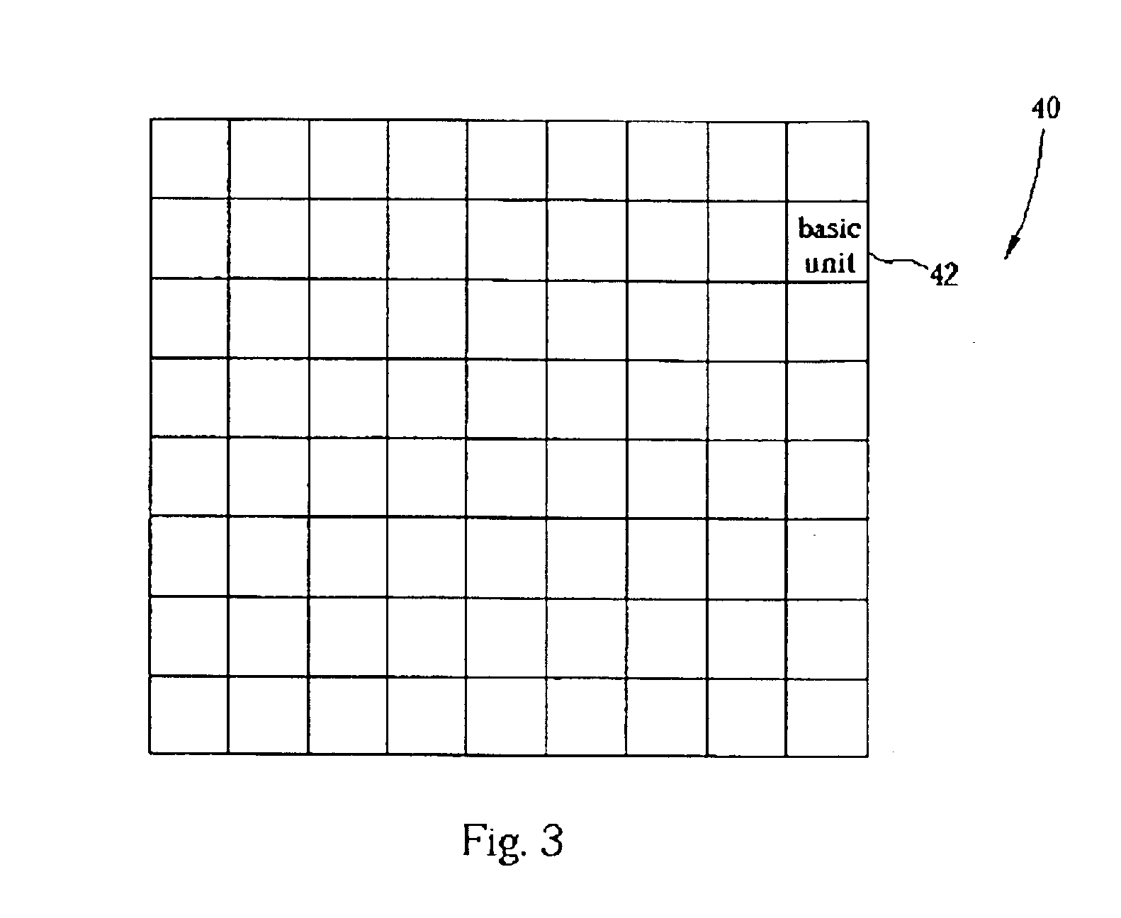
[0043]Please refer to FIG. 3, which is a diagram showing a semiconductor body 40 according to the present invention. The semiconductor body 40 has a plurality of basic units 42. In the preferred embodiment, the basic units 42 are positioned on the semiconductor body 40 according to a matrix format for acquiring greater density. In other words, the area required to accommodate the basic units 42 is reduced to further shrink size of the corresponding integrated circuit. However, the basic units 42 can be position on the semiconductor body 40 according to other arrangements. For example, the basic units 42 are positioned in the same row or in the same column to be an array.

[0044]A semiconductor foundry fabricates the semiconductor body 40 in advance. An integrated circuit designer is then capable of designing photomask patterns for traces routed among the basic units 42. In the end, according to the photomask patterns designed by the integrated circuit designer, the semiconductor found...


PUM


Abstract

A method for forming a metal programmable integrated circuit that can use a plurality of clock sources and balance clock skew. The integrated circuit has a semiconductor body. The method includes step (a) used for forming a plurality of basic units on the semiconductor body wherein each basic unit has at least a logic module, at least a driving module, and at least a storage module, and step (b) used for forming a metal layer for programming the logic module to be able to perform logic operations, programming the driving module to able to drive an input signal inputted into the driving module, and programming the storage module to be able to store data after performing step (a).

Description

BACKGROUND OF INVENTION[0001]1. Field of the Invention[0002]The present invention relates generally to a metal programmable integrated circuit and a related method for forming the metal programmable integrated circuit. More specifically, the present invention discloses a metal programmable integrated circuit capable of utilizing a plurality of clock sources and capable of eliminating clock skew and a related method for forming the metal programmable integrated circuit.[0003]2. Description of the Prior Art[0004]In the past, electronic components such as capacitors and resistors are electrically connected with the help of a rigid circuit board. However, semiconductor technology advances integrated circuits. That is, well-known electronic components are fabricated on one chip and the required traces connecting the well-known electronic components are implemented according to the same semiconductor technology.[0005]Recently, the semiconductor technology process has developed to utilize ...

Claims


Application Information

Patent Timeline
Patent Type & Authority Patents(United States)
IPC IPC(8): H01L21/70H01L21/82G06F1/10H01L27/118
CPCG06F1/10H01L27/11803
Inventor WANG, HSIN-SHIHSHIEH, SHANG-JYH
Owner FARADAY TECH CORP
Why Eureka
Try Eureka