SRAM cell and method of manufacturing the same

a random access memory and cell technology, applied in semiconductor devices, digital storage, instruments, etc., can solve the problems of soft error, electric charge stored in a cell node to be lost, soft error, etc., and achieve the effect of reducing soft error and increasing cell capacitan

Active Publication Date: 2005-06-07
SK HYNIX INC
View PDF8 Cites 8 Cited by
  • Summary
  • Abstract
  • Description
  • Claims
  • Application Information

AI Technical Summary

Benefits of technology

[0026]According to the present invention, capacitance is additionally formed to increase cell capacitance, so that variation of the electric potentials of cell nodes, which is caused by generated electrons, is prevented, and thereby soft error can be efficiently reduced.

Problems solved by technology

Recently, with the improvement of technology and density of a memory cell and the decrease of the operation voltage, the soft error rate has emerged as a hot issue.
The “soft error rate” refers to the discordance between written information and read information in / from a memory cell, that is, a fault caused by information loss.
That is, when alpha particles pass a storage area of a cell, charge Up-set is generated to cause electric charge stored in a cell node to be lost.
As a result, the actual stored information changes, thus causing soft error.
Therefore, node voltage is varied, so that soft error is caused.
Such soft errors have actually emerged as a big problem in SRAM cells, and a number of studies have been made to solve this problem.

Method used


Image

  • SRAM cell and method of manufacturing the same
  • SRAM cell and method of manufacturing the same
  • SRAM cell and method of manufacturing the same

Examples


Embodiment Construction

[0034]Hereinafter, a preferred embodiment of the present invention will be described in detail.

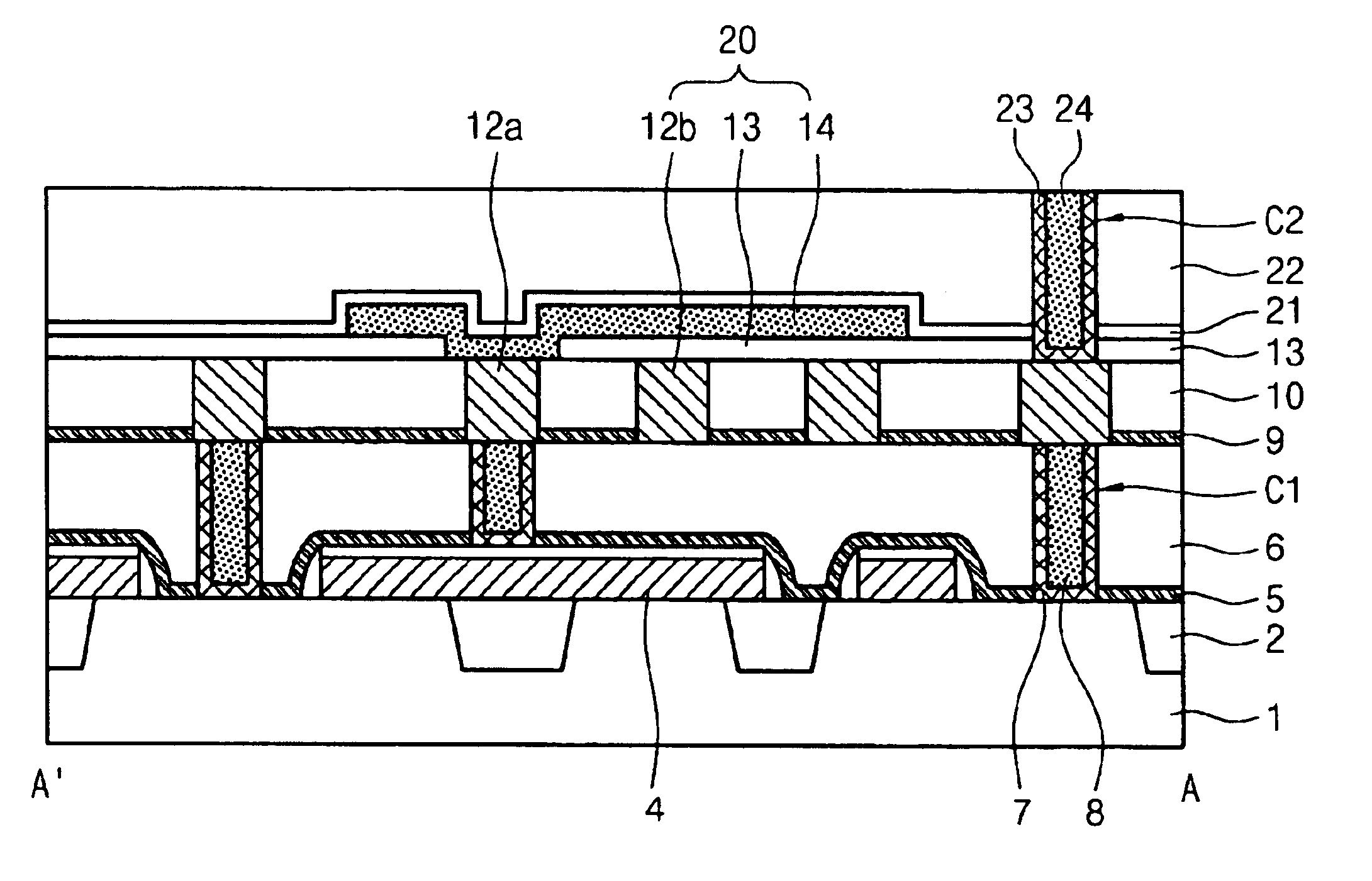
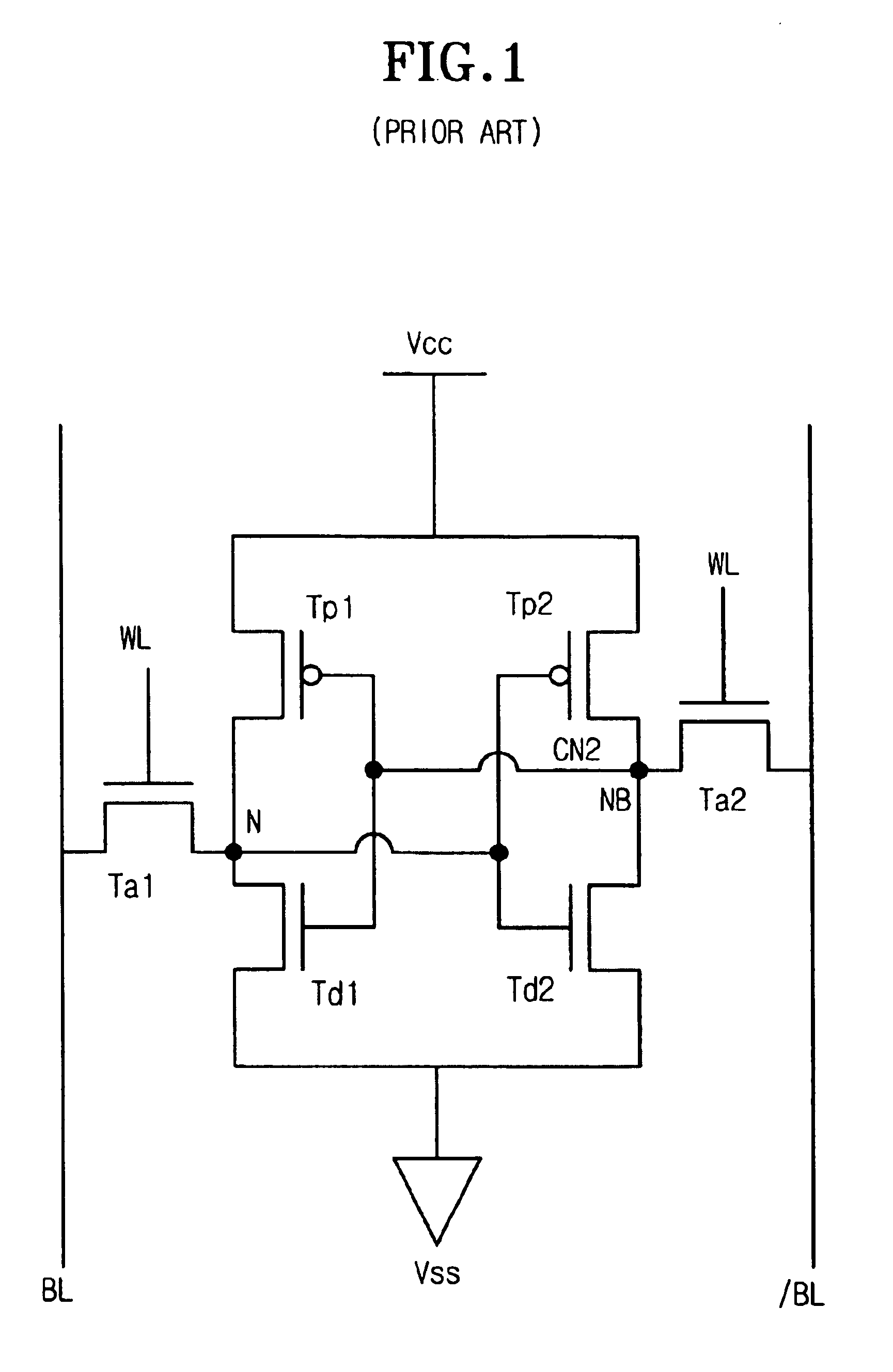
[0035]The soft error in a SRAM, as described above, is caused by variation of a node voltage which is generated so that electrons having arrived at a cell node change the electric charge distribution of the cell node. If the amount of electric charge in a cell node, which may vary the node voltage, is increased, the variation of a node voltage caused by electrons having arrived at the cell node is inhibited, and thereby soft error can be efficiently reduced.

[0036]Therefore, in the present invention, cell capacitance is increased to increase the amount of electric charge in a cell node, so that undesired variation of a node voltage caused by electrons having arrived at the cell node is prevented, and thereby the soft error rate is reduced. To this end, in the present invention, after metal interconnection lines are formed, a dielectric film and a metal plate are formed, and thereby addition...


PUM


Abstract

Disclosed is a SRAM cell and a method of manufacturing the same. The SRAM cell comprises: a pair of access devices; a pair of pull-up devices; a pair of pull-down devices; and at least one metal plate formed on metal interconnection lines in contact with a substrate, having a dielectric film interposed between the metal plate and the metal interconnection lines, so as to increase a cell capacitance, thereby reducing a soft error rate. Herein, one metal plate may be included in each cell. In this case, the metal plate overlaps with a first one of metal interconnection lines of a node side and a node bar side, while being in contact with a second one of the metal interconnection lines of the node side and the node bar side. Also, two metal plates may be included in each cell. In this case, the metal plates overlap, respectively, with one metal interconnection line of metal interconnection lines of a node side and a node bar side, while being in contact with another metal interconnection line of the node side or the node bar side, respectively. Therefore, capacitance is additionally formed to increase cell capacitance, so that variation of the electric potentials of cell nodes, which is caused by generated electrons, is prevented, and thereby soft error can be efficiently reduced.

Description

BACKGROUND OF THE INVENTION[0001]1. Field of the Invention[0002]The present invention relates to a static random access memory (SRAM), and more particularly to an SRAM cell which can reduce a soft error rate and a method of manufacturing the same.[0003]2. Description of the Prior Art[0004]An SRAM is a memory device which is driven at a high speed, at a low power, and in a simple manner. The SRAM is advantageous in that a periodical refresh of stored information is not required, unlike a dynamic random access memory (DRAM), and also designing is easy.[0005]Such an SRAM comprises a pair of access-devices for cell selection, a pair of pull-down devices functioning as driving devices, a pair of pull-up devices functioning as load devices. Herein, the pull-up devices are classified into three types, that is, a Full CMOS type, a High Load Resistor type, and a Thin Film Transistor type, according to their structure.[0006]FIG. 1 is a circuit diagram of a conventional Full CMOS-type SRAM cel...

Claims


Application Information

Patent Timeline
Patent Type & Authority Patents(United States)
IPC IPC(8): H01L29/76H01L21/00H01L21/70H01L29/66H01L21/84G11C11/412H01L21/8244H01L27/11
CPCG11C11/412H01L27/1104H01L27/11H10B10/00H10B10/12H10B99/00
Inventor KIM, DO WOOLEE, CHANG YEOLGONG, MYEONG KOOK
Owner SK HYNIX INC
Why Eureka
Try Eureka