Method of purging semiconductor manufacturing apparatus and method of manufacturing semiconductor device

a technology of manufacturing apparatus and semiconductor, which is applied in the direction of chemistry apparatus and processes, cleaning of hollow objects, coatings, etc., can solve the problems of cvd films formed over semiconductor wafers that are not uniform, the inside of the chamber is thereby contaminated, and the peeling of films, etc., to shorten the purging time, increase the efficiency of the apparatus, and increase the efficiency

Inactive Publication Date: 2005-06-07
KK TOSHIBA
View PDF14 Cites 27 Cited by
  • Summary
  • Abstract
  • Description
  • Claims
  • Application Information

AI Technical Summary

Benefits of technology

[0010]The present invention is made under the circumstances described above, and it is an object of the invention to provide a method of purging a semiconductor manufacturing apparatus such as a CVD apparatus by shorting purge time to increase the rate of apparatus operation and increase the productivity and to provide a method of manufacturing a semi-conductor device using a semiconductor manufacturing apparatus purged by the purging method.

Problems solved by technology

When such a CVD-deposited film is formed excessively thick, a problem occurs that peel of the film occurs, and inside of the chamber is thereby contaminated.
In addition, when the film peel has occurred to make the thickness of deposited films in the chamber non-uniform, CVD films formed over semiconductor wafers are not formed to be uniform.
However, since the etching gas such as ClF3 contains halogen of high electronegativity, then the etching gas adsorbed in the chamber surface can not be sufficiently desorbed through a short-time purge treatment.
As the result, conventionally, a long-time purge treatment has been required.
However, in a CVD mode in which cleaning needs to be performed every time a CVD process is performed, long purge time leads to a reduction in the throughput.

Method used


Image

  • Method of purging semiconductor manufacturing apparatus and method of manufacturing semiconductor device
  • Method of purging semiconductor manufacturing apparatus and method of manufacturing semiconductor device

Examples


first embodiment

[0020]A first embodiment will be described with reference to FIG. 1.

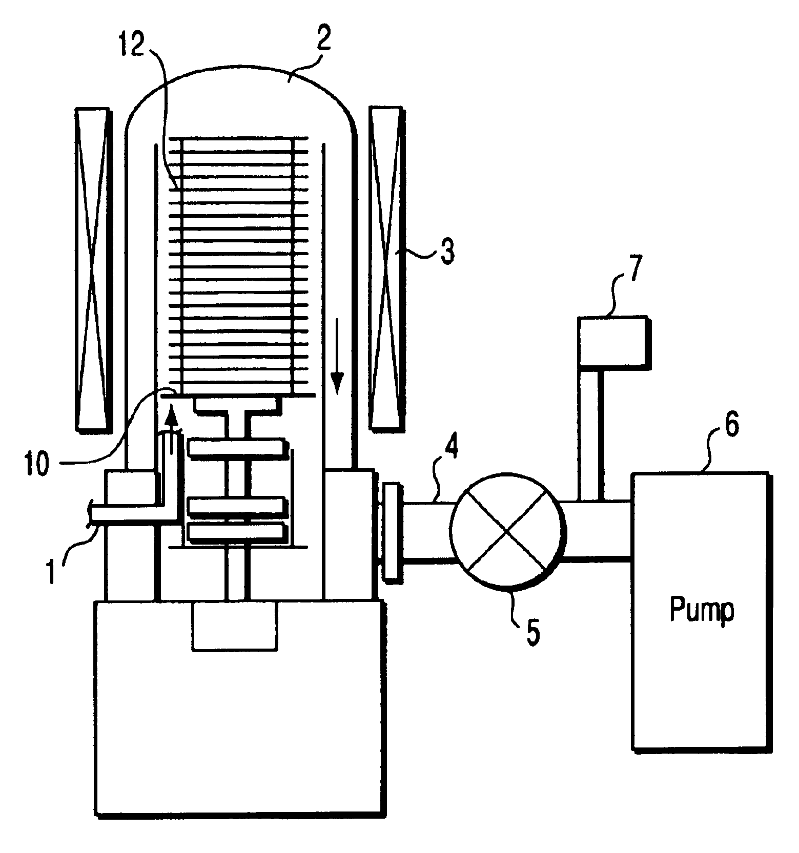
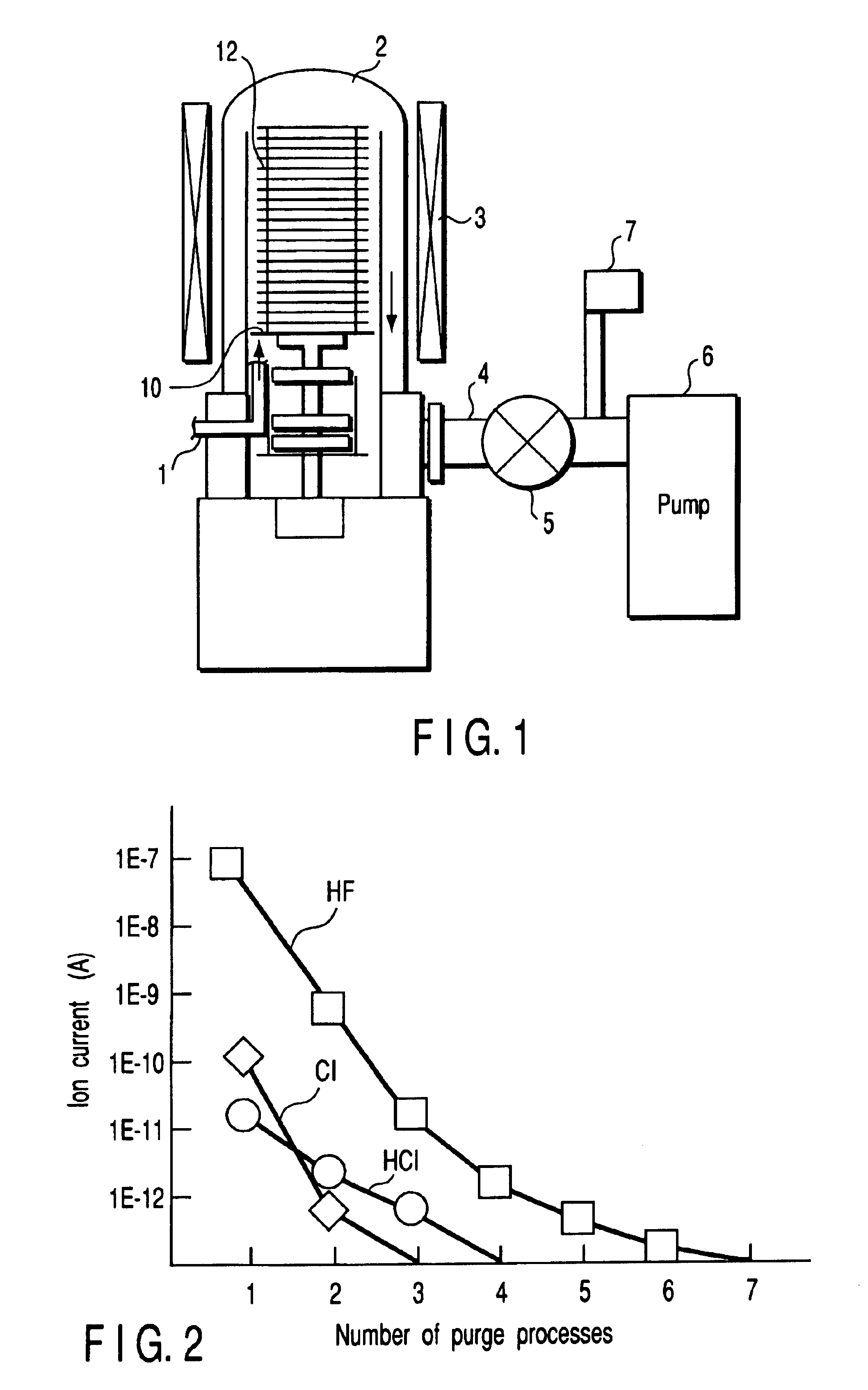
[0021]FIG. 1 shows a schematic cross-sectional view of a vertical type CVD apparatus, which is used as a semiconductor manufacturing apparatus. A boat 10 is provided in a vertical type chamber 2, and semi-conductor wafers 12 such as silicon wafers are mounted on the boat prior to a CVD process. A gas inlet 1 is mounted on a lower portion of the chamber 2, and a cleaning gas is introduced into the chamber 2 through the gas inlet, upon operation of a mass-flow control valve (not shown). A heater 3 is disposed in an outer portion of the chamber 2 to heat semiconductor wafers 12 mounted on the boat 10. The chamber 2 is connected to a pump 6 via an exhaust tube 4 having a pressure control valve 5, in which operation of the pressure control valve 5 exhausts the chamber to appropriate pressure.

[0022]Using the CVD apparatus shown in FIG. 1, a silicon film was formed by an LP-CVD process over the semi-conductor wafers 12 pro...

second embodiment

[0028]Hereinafter, the present invention will be described.

[0029]Also in this embodiment, cleaning was performed using the ClF3 gas for the inside of a chamber in a state where a silicon film is deposited to the inside of the chamber, as in the first embodiment.

[0030]The purge after the cleaning was performed with a mixed gas of 5 slm nitrogen and 25 sccm water-vapor (H2O). The chamber pressure at the time was 100 Torr, and hence the water-vapor partial pressure was 0.5 Torr (i.e. 0.5 mmHg). Similarly to the case of the first embodiment, the purge cycle of the exhausting step and the gas supply step was repeated five times in total for comparison. When monitoring is made using the Q-mass spectrometer, it was confirmed that residual gases such as HCl and HF, which are considered attributable to the ClF3 gas, were not present.

[0031]For comparison, in a case where alone nitrogen was caused to flow, it was confirmed that HF and HCl remained with the same number of purge cycles (5 times)...

third embodiment

[0038]Hereinafter, the present invention will be described.

[0039]Also in this embodiment, cleaning was performed using the ClF3 gas for the inside of the chamber in a state where a silicon film is deposited to the inside of the chamber, as in the first embodiment.

[0040]A purge process after the cleaning was performed with a mixed gas of 2 slm nitrogen and a 500 sccm ammonia (NH3). The purge cycle of the exhausting step and the gas supply step was repeated three times in total for comparison. When monitoring was performed using the Q-mass spectrometer, then it was confirmed that residual gases such as HCl and HF, which are considered attributable to the ClF3 gas, were not present at all.

[0041]In the present embodiment, while the ammonia flow rate was set to 500 sccm, it may be set to a range of from 100 sccm to 2 slm, in which the addition effect can be exhibited. Similarly, while the nitrogen flow rate was set to 2 slm in the present embodiment, it may be in a range of from 10 sccm ...


PUM

PropertyMeasurementUnit
temperatureaaaaaaaaaa
pressureaaaaaaaaaa
temperatureaaaaaaaaaa

Abstract

A method of purging a semiconductor manufacturing apparatus comprises a step of etching a CVD-deposited film deposited in a chamber constituting a semiconductor manufacturing apparatus which has performed a process of forming a CVD film using a CVD process over a semiconductor wafer by using an etching gas containing at least a halogen gas, and a step of purging a cleaning gas remaining in the chamber by causing a gas containing hydrogen to flow into the chamber after the step of etching the CVD-deposited film by using the cleaning gas.

Description

CROSS-REFERENCE TO RELATED APPLICATIONS[0001]This is a Continuation Application of PCT Application No. PCT / JP02 / 08742, filed Aug. 29, 2002, which was not published under PCT Article 21 (2) in English.[0002]This application is based upon and claims the benefit of priority from the prior Japanese Patent Application No. 2001-262295, filed Aug. 30, 2001, the entire contents of which are incorporated herein by reference.BACKGROUND OF THE INVENTION[0003]1. Field of the Invention[0004]The present invention relates to a process of purging a semiconductor manufacturing apparatus, more specifically, to a purge step for a CVD (chemical vapor deposition) apparatus after dry-cleaning step.[0005]2. Description of the Related Art[0006]When a semiconductor manufacturing apparatus, for example, a CVD apparatus such as a LP (low pressure)-CVD apparatus is used, silicon, silicon oxides, silicon nitrides, and / or thin-film materials to be used in a semiconductor device are deposited within a reaction ch...

Claims


Application Information

Patent Timeline
Patent Type & Authority Patents(United States)
IPC IPC(8): C23C16/44H01L21/205
CPCC23C16/4405C23C16/4412C23C16/4408Y10S438/905H01L21/205
Inventor MIZUSHIMA, ICHIRO
Owner KK TOSHIBA
Why Eureka
Try Eureka