Method for preventing the etch transfer of sidelobes in contact hole patterns

Inactive Publication Date: 2005-06-14
TAIWAN SEMICON MFG CO LTD
View PDF12 Cites 53 Cited by
  • Summary
  • Abstract
  • Description
  • Claims
  • Application Information

AI Technical Summary

Benefits of technology

[0018]One objective of the present invention is to provide a method of preventing sidelobes

Problems solved by technology

The patterning of contact holes for current and next generation devices is a difficult challenge for lithography engineers.
A major concern is the inadequate DOF for small contact holes.
Unfortunately, these methods induce a sidelobe pattern in the photoresist and surface damage that will cause damage to the device during a subsequent etch transfer step.
However, since sidelobe 18 extended deep into photoresist 11, the film thickness below sidelobe 18 was not suffi

Method used


Image

  • Method for preventing the etch transfer of sidelobes in contact hole patterns
  • Method for preventing the etch transfer of sidelobes in contact hole patterns
  • Method for preventing the etch transfer of sidelobes in contact hole patterns

Examples


first embodiment

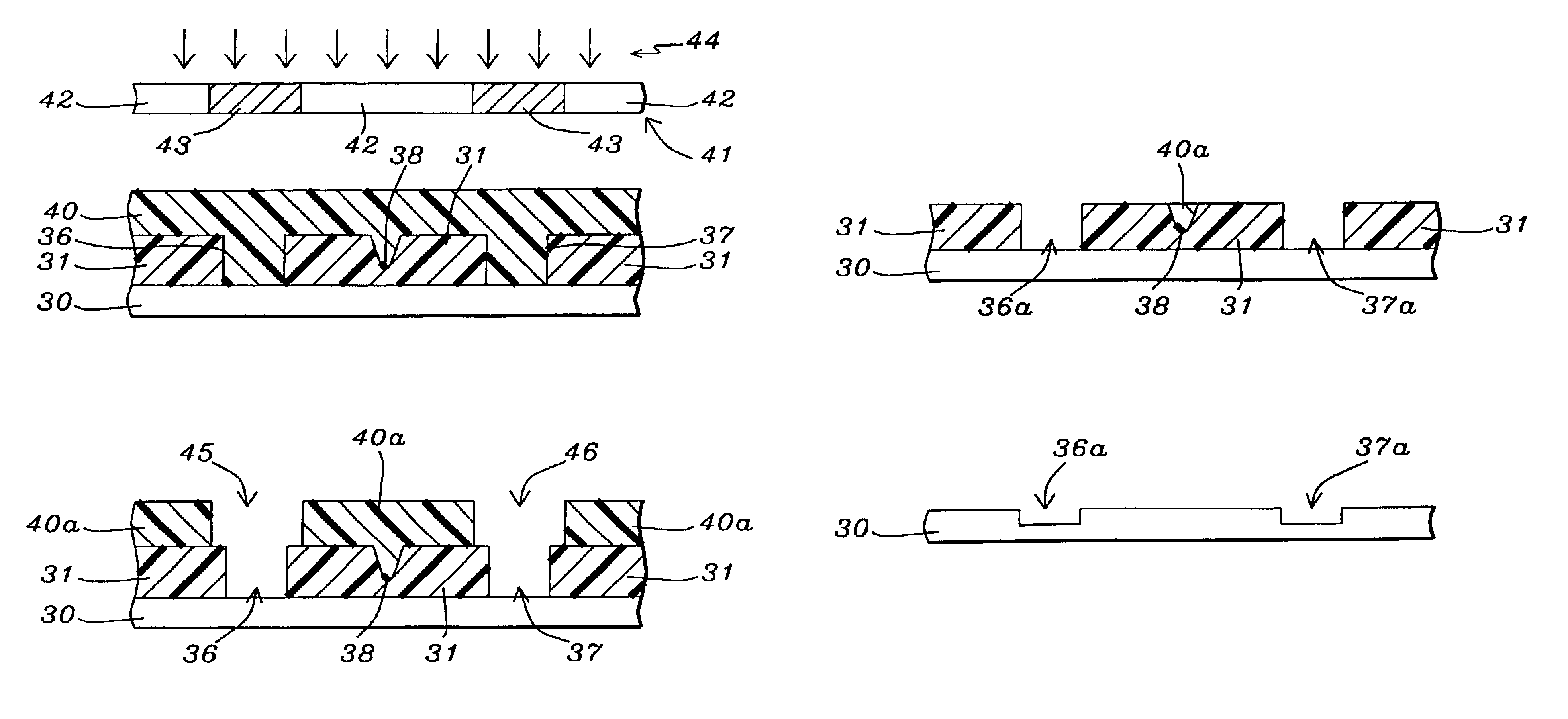
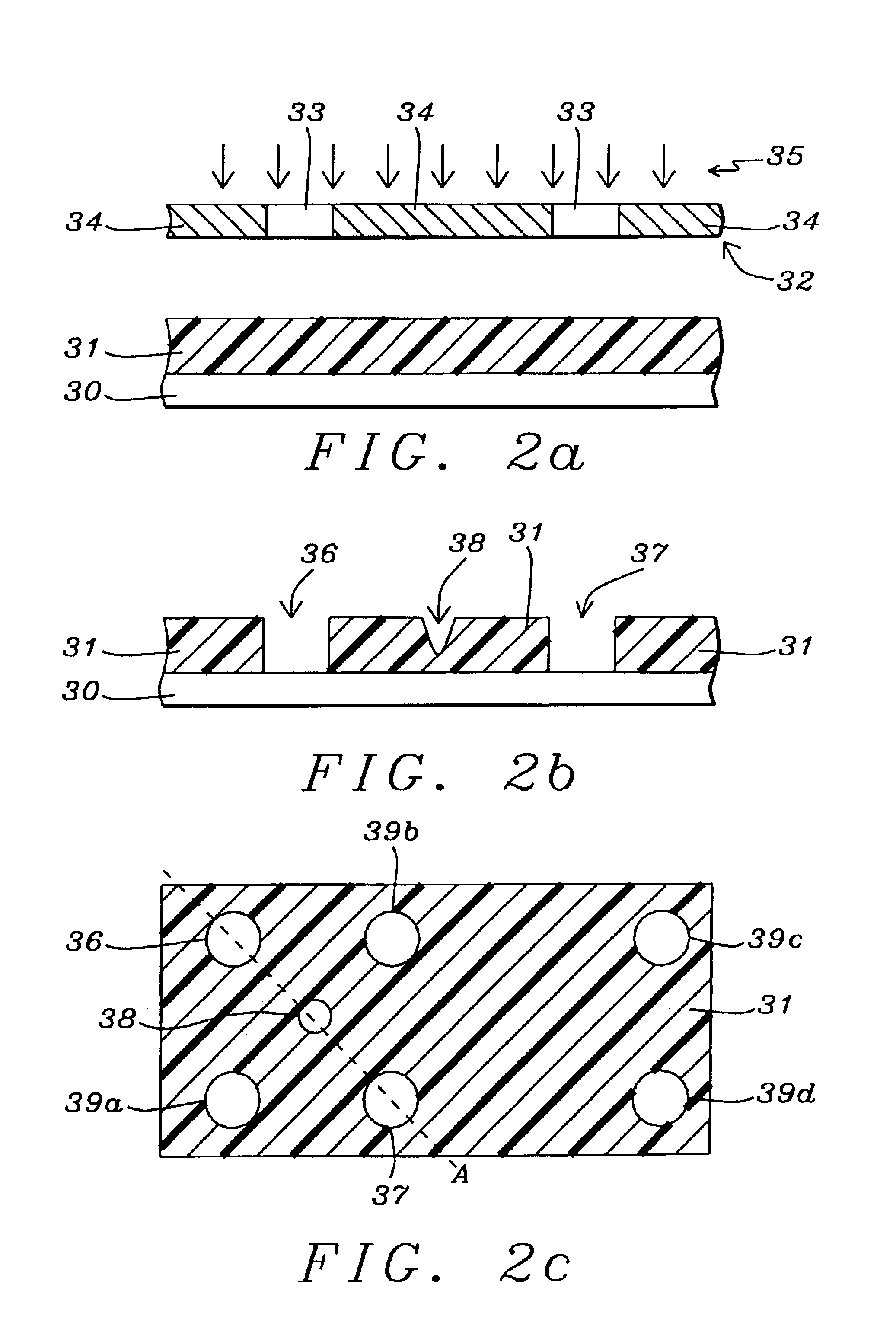
[0031]In the first embodiment as illustrated in FIGS. 2a-2f, a substrate 30 is provided that typically contains active and passive devices in a substructure that is not shown in order to simply the drawing and direct attention to the present invention. Optionally, an anti-reflective coating or ARC (not shown) is formed on substrate 30 in order to control reflectivity during a subsequent photoresist patterning process. The ARC can be an inorganic material like silicon nitride or silicon oxynitride that is deposited by a chemical vapor deposition (CVD) process or the ARC can be an organic layer that is obtained by spin coating and baking a commercially available material. A typical thickness for an ARC is between about 300 and 1000 Angstroms.

[0032]Referring to FIG. 2a, a positive tone photoresist from a commercial supplier is spin coated and baked to form photoresist layer 31 which normally has a thickness in the range of about 2000 to 10000 Angstroms. The photoresist thickness is usu...

second embodiment

[0045]In a second embodiment, a substrate 50 as depicted in FIG. 3a is provided that typically contains active and passive devices in a substructure that is not shown in order to simply the drawing and direct attention to the present invention. An anti-reflective coating or ARC 51 having a thickness between about 300 to about 1000 Angstroms is formed on substrate 50 in order to control reflectivity during a subsequent photoresist patterning process. The ARC 51 can be an inorganic material like silicon nitride or silicon oxynitride that is deposited by a chemical vapor deposition (CVD) process or the ARC can be an organic layer that is obtained by spin coating and baking a commercially available material. If ARC 51 is an organic material, its selection depends on the type of photoresist 52 and exposure wavelength 56 used in the patterning step. Normally, the refractive index (n and k) and thickness of ARC 51 is tuned to minimize reflectivity of the exposing radiation and is determine...


PUM

PropertyMeasurementUnit
Thicknessaaaaaaaaaa
Thicknessaaaaaaaaaa
Thicknessaaaaaaaaaa

Abstract

A method is provided for removing sidelobes that are formed when patterning a positive photoresist layer with an Att. PSM, Alt. PSM or a binary mask with scattering bars. A water soluble negative tone photoresist is coated over the positive photoresist pattern and is exposed through a mask having small islands that correspond in shape, size and location to the small holes in the mask used to pattern the positive tone photoresist. After development, exposed negative tone photoresist covers sidelobes formed by the positive tone process. The negative tone photoresist functions as a mask for a subsequent etch transfer of the positive tone pattern into the substrate. A method of aligning openings in a positive tone pattern over the same openings in a negative tone pattern is also useful in preventing sidelobes in the positive tone photoresist from being transferred into the substrate.

Description

FIELD OF THE INVENTION[0001]The invention relates to a method of fabricating an integrated circuit in a semiconductor device. More particularly, the present invention relates to a method of forming a pattern in a substrate that is free of surface damage or divots caused by an etch transfer of sidelobes from a photoresist layer.BACKGROUND OF THE INVENTION[0002]Photoresist patterning is a key step in the formation of integrated circuits in semiconductor devices. A photoresist layer is typically spin coated on a substrate and patternwise exposed by employing an exposure tool and a mask that contains a device pattern. Radiation is transmitted through transparent regions of the mask to selectively expose portions of the photoresist layer which are later developed in a media such as aqueous base to produce a photoresist pattern on the substrate. Each technology generation or node in the microelectronics industry is associated with a particular minimum feature size in the photoresist patte...

Claims


Application Information

Patent Timeline
IPC IPC(8): G03F7/00H01L21/02H01L21/027
CPCH01L21/0274G03F7/0035
Inventor HO, BANG-CHEINCHEN, JIAN-HONG
Owner TAIWAN SEMICON MFG CO LTD
Why Eureka
Try Eureka