Method and apparatus for self-referenced dynamic step and scan intra-field scanning distortion

a dynamic step and scanning technology, applied in the field of semiconductor manufacturing, can solve the problems of affecting the accuracy of the alignment accuracy of the exposure tool system, affecting the performance of the photolithographic system, and affecting the calibration procedure of the exposure tool,

Inactive Publication Date: 2005-06-14
LITEL INSTR
View PDF16 Cites 21 Cited by
  • Summary
  • Abstract
  • Description
  • Claims
  • Application Information

AI Technical Summary

Problems solved by technology

Intra-field overlay errors are generally composed of lens aberrations or distortions, scanning irregularities, and reticle alignment
Inaccurate overlay modeling algorithms can corrupt the exposure tool calibration procedures and degrade the alignment accuracy of the exposure tool system.
Today, these photolithographic systems are pushed to performance limits.
The resulting overlay error at each field position can be measured with a standard optical overlay tool and the result is interpreted as being intra-field error.
A problem with this technique is two-fold, first, it is standard practice to assume that the wafer stage error is very small, randomly distributed, and can be completely accounted for using a statistical model.
In general, positional uncertainties in the wafer stage introduces both systematic and random errors, and since the intra-field distortion is measured only in reference to the lithography tool's wafer stage, machine to machine wafer stage differences show up as inaccurate intra-field distortion maps.
Secondly, the assumption that lens distortion is zero at the center of the lens incorrect.
Furthermore, the model represented by Equations 1 and 2 is entirely unsuited to modeling scanner overlay error—typically the intra-field distortion model accounts only for scanner skew and scanner scale overlay errors—in general, the synchronization errors between the reticle stage and wafer stage introduce more complex errors described below.
This technique has several drawbacks, including that it requires that the measurements be performed on the same machine that is being assessed by this technique.
Another drawback to these techniques to determine intra-field error is that they use the scanner itself as the metrology tool.

Method used


Image

  • Method and apparatus for self-referenced dynamic step and scan intra-field scanning distortion
  • Method and apparatus for self-referenced dynamic step and scan intra-field scanning distortion
  • Method and apparatus for self-referenced dynamic step and scan intra-field scanning distortion

Examples


first embodiment

A FIRST EMBODIMENT

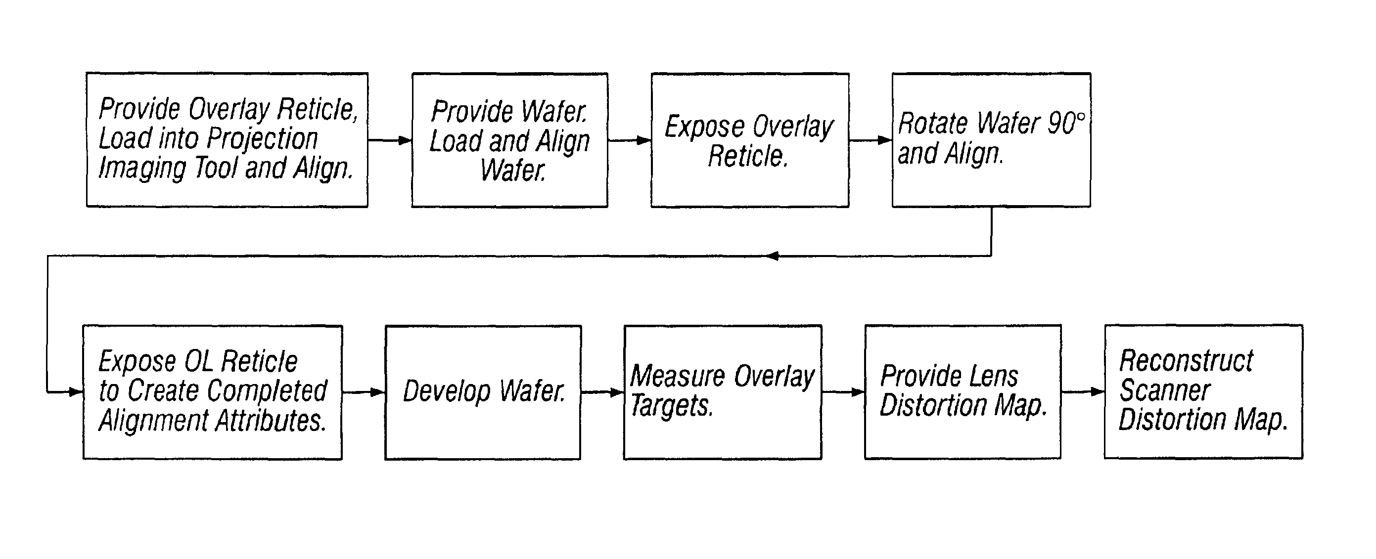
[0092]A method for determining the distortion associated with scanner synchronization error (scan error for short) to within a translation, rotation, and skew in the presence of scanner lens distortion is described. The process flow for the first embodiment is diagramed in FIG. 12.

Provide Reticle

[0093]Referring to FIG. 6, a reticle, OL, with an (Mx×My) array of overlay groups, OG, is provided, loaded into a projection lithography tool (machine) being Measuring, and aligned to reticle alignment mark RM. Reticle OL, shown in cross section in FIG. 11, may be a glass or fused silica reticle with a chrome coating that defines the overlay groups, OG; it is a binary mask. FIGS. 7 and 9 show realizations of OG for the first embodiment. They both consist of alignment attributes, AA, and complementary alignment attributes, AA′, offset from AA a distance M*dp. When overlaid one on top of another, AA and M′ form completed alignment attributes, CAA, illustrated in FIGS. 8 and 1...

second embodiment

[0123]Instead of the reticle of FIG. 6, this invention could be carried out with the reticle layout of FIG. 13. It too consists of an Mx×My array of overlay groups OG on regular pitch M*p″ the only difference being in the details of the overlay group. Now overlay group OG consists of alignment attribute AA and only a single complementary alignment attribute, AA′, offset from it in a single direction. An example of an overlay group with this structure is shown in FIG. 21. There a dark field reticle design consists of outer bar alignment attribute AA and the complementary alignment attribute consists of an inner bar alignment attribute AA′. Reticle dimensions suitable for an M=4 or 5 reduction imaging lithography tool are shown. FIG. 22 shows how projected overlapped overlay groups OLAP1, OLAP2 and OLAP of FIG. 18 would appear when the overlay group of FIG. 21 is utilized. Lower, CAAL, and upper, CAAU, completed alignment attributes are also indicated. The dark areas correspond to exp...

third embodiment

[0124]In this case, the overlay groups OG of reticle OL (FIG. 6) consist of a pair of wafer alignment marks. Referring to FIG. 23, overlay group OG consists of alignment attribute AA and offset from it is complementary alignment attribute AA′. AA is a wafer alignment mark, WAM0, suitable for use by a lithography tool wafer alignment system and stage when the wafer is in the nominal or 0 degree position. AA′ is a wafer alignment mark, WAM90, which is wafer alignment mark WAM0 rotated by 90 degrees in a clockwise direction. FIG. 24 shows how projected overlapped overlay groups OLAP1, OLAP2 and OLAP of FIG. 18 would appear when the overlay group of FIG. 23 is utilized. Lower, CAAL, and upper, CAAU, completed alignment attributes are also indicated. The exposure steps of the preferred embodiment must be altered is an obvious way so the wafer pattern results in the projected overlapped overlay groups OLAP1, OLAP2 and OLAP of FIG. 24. The other step that differs in detail is that of measu...


PUM

PropertyMeasurementUnit
distancesaaaaaaaaaa
distancesaaaaaaaaaa
sizeaaaaaaaaaa

Abstract

A method and apparatus for determining the dynamic scanning distortion present in lithographic scanners. A special reticle pattern is exposed over the full field that is to be characterized. The wafer is then rotated 90 degrees and one or more exposures over the same field are made. Interlocking alignment structures on the resulting developed wafer are then measured and used to reconstruct the dynamic scanner distortion to within a translation, rotation, and scan skew. Alternative embodiments describe techniques for extracting the repeatable part of the dynamic scan error.

Description

REFERENCE TO PRIORITY DOCUMENT[0001]This application claims the benefit of priority of co-pending U.S. Provisional Patent Application Ser. No. 60 / 323,577, entitled “Method for Self-Referenced Dynamic Step and Scan Intra-Field Scanning Distortion”, by Adlai Smith, filed Sep. 20, 2001. Priority of the filing date of Sep. 20, 2001 is hereby claimed, and the disclosure of the Provisional Patent Application is hereby incorporated by reference.BACKGROUND OF THE INVENTION[0002]1. Field of the Invention[0003]The present invention relates generally to processes for semiconductor manufacturing and more particularly to characterizing and monitoring the intra-field distortions of scanning projection systems used in ULSI photolithography.[0004]2. Description of the Related Art[0005]Today's lithographic processing requires ever tighter layer-to-layer overlay toleranccs to meet device performance requirements. Overlay registration on critical layers can directly impact device performance, yield an...

Claims


Application Information

Patent Timeline
Patent Type & Authority Patents(United States)
IPC IPC(8): G01B9/00H01L27/00G03F7/20G03F9/00H01J37/317
CPCB82Y10/00B82Y40/00G03F9/7011H01J37/3175G03F7/70358H01J2237/3045
Inventor SMITH, ADLAI
Owner LITEL INSTR
Why Eureka
Try Eureka