Remote wafer flow and recipe editor for simiconductor processing control

a technology of simiconductor and processing control, applied in the field of simiconductor processing, can solve the problems of affecting the quality of the final product, so as to achieve the effect of reducing the difficulty of comparing the recipe file of the track controller with the master track file, and saving valuable production tim

Inactive Publication Date: 2005-06-14
ADVANCED MICRO DEVICES INC
View PDF17 Cites 36 Cited by
  • Summary
  • Abstract
  • Description
  • Claims
  • Application Information

AI Technical Summary

Benefits of technology

[0013]The editor system may further communicate with multiple track controllers or host controllers that are remotely located within a fabrication clean room, each through a SECS / GEM interface, and operate on multiple track controllers simultaneously. The editor system may further access local, remote, and host controller recipe and flow databases. The editor edits flows and recipes without interrupting the process track and correctly renumbers line and flow numbers of the recipes when editing, deleting, or inserting process steps. The editor can further perform side-by-side comparisons of multiple recipes, verify the contents of the track recipe files with master recipes, and provide indicators of mismatches. The editor allows one to copy, rename, and print recipes. Finally, the editor allows one to export and import recipes to and from remote recipe databases.

Problems solved by technology

Editing recipes at the processing tool controller requires that the processing tool be taken off-line because editing a recipe during production can cause faulty processing of the wafer and defects in the final product.
When a processing tool is taken off-line valuable production time is lost.
A further problem with existing track editors is that it is difficult and time consuming to compare recipe files of the track controller with the master track files to ensure the proper recipes are running on a given processing tool.
In addition to employing someone to ensure proper recipe contents, this down time of the processing tool is a costly burden upon the output production.
Further, current track editors have limited intelligence that may lead to costly errors when editing recipes.
Manually updating the line numbers and / or flow line steps is a time consuming task and can lead to costly errors in the fabrication of semiconductor devices.
Existing editors also fail to provide the ability to easily manipulate flows and recipes.

Method used


Image

  • Remote wafer flow and recipe editor for simiconductor processing control
  • Remote wafer flow and recipe editor for simiconductor processing control
  • Remote wafer flow and recipe editor for simiconductor processing control

Examples


Embodiment Construction

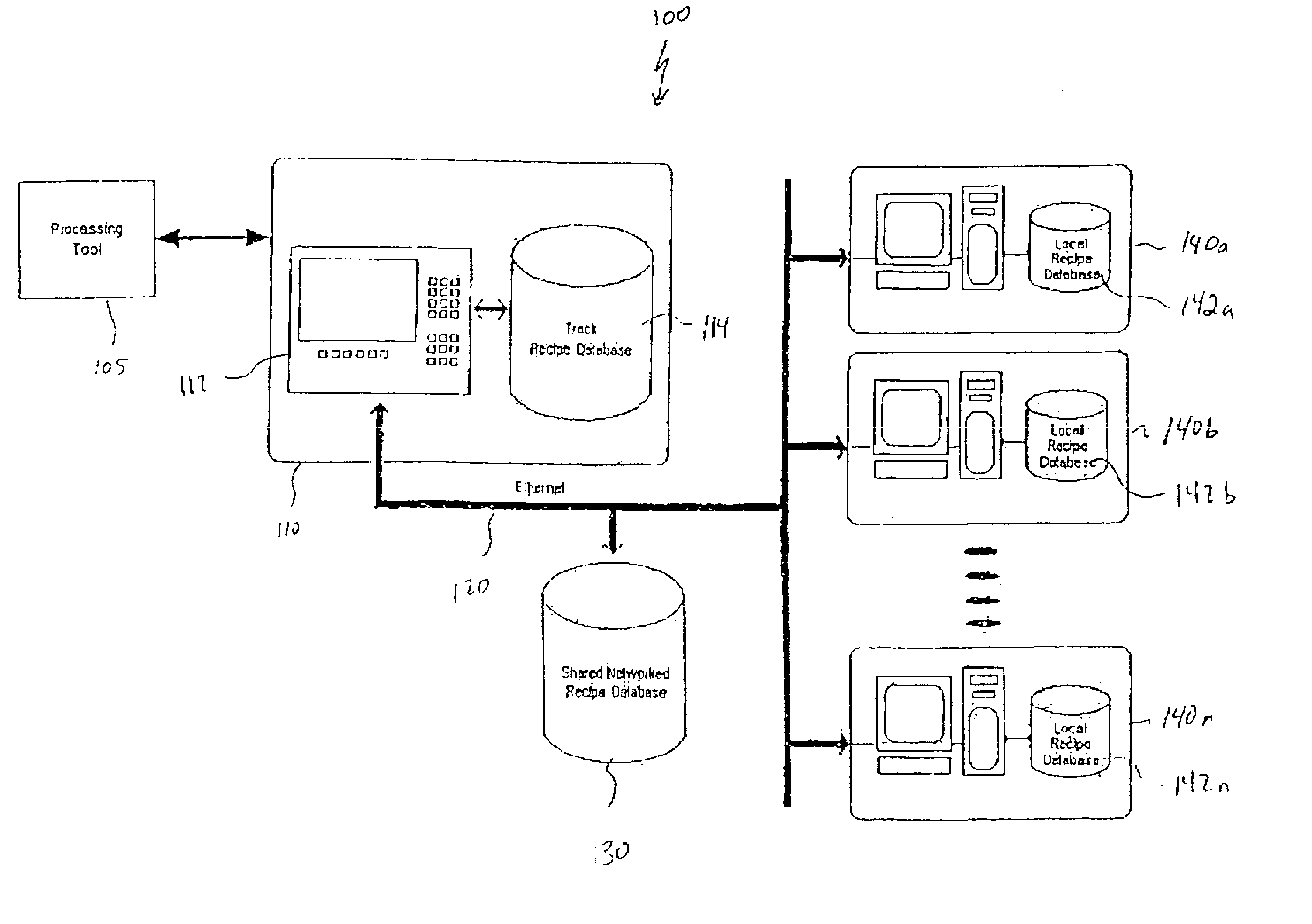
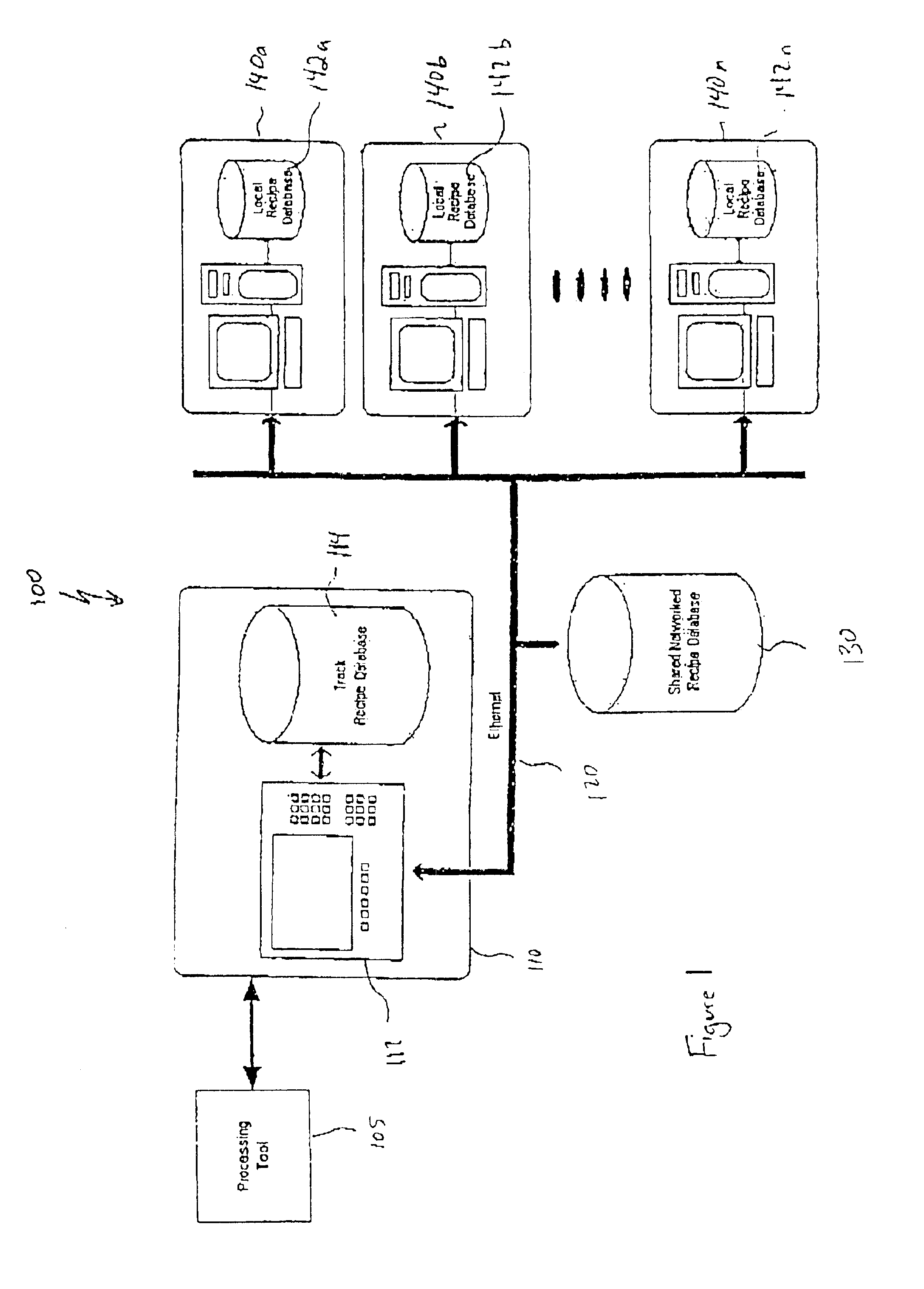
[0034]In accordance with the present invention, a method and system are provided for remotely editing, updating, copying, and verifying process flow and recipes of multiple semiconductor processing tools without interfering with the operation of the processing equipment, and further offering greater opportunities for manipulating recipe data. The editing system remotely edits multiple processing tools allowing one to quickly update flows and recipes for multiple processing tools from a single remote location. Further, remote access allows control of the processing equipment remotely (i.e., through an Intranet or Internet connection). Remote access also allows for different facilities located in different locations around the world to share and compare recipes. A more secure back-up storage of recipes is also provided that allows for quickly verifying the content of track recipe files to master recipe files. Further, remote access allows for greater storage of multiple recipes within...


PUM


Abstract

A remote track editor system, method, and computer readable medium is provided to remotely edit track flows and recipes of semiconductor processing tools. The editor system includes a processing track, a track controller, and a remote track editor for remotely editing recipes of at least one semiconductor processing tool. The editor system communicates with remote terminals and accesses multiple flows and recipes stored on network databases through a SECS/GEM interface. The remote track editor edits recipes without interrupting the process track and correctly renumbers line and flow numbers of the recipes when editing, deleting, or inserting steps. The remote track editor also performs side-by-side comparisons of multiple recipes, verifies the contents of recipes to master recipes, and provides indicators of mismatches.

Description

BACKGROUND OF THE INVENTION[0001]1. Field of the Invention[0002]This invention relates to semiconductor processing, and more particularly to wafer flow and recipe editing for control of semiconductor processing equipment.[0003]2. Description of the Related Art[0004]The fabrication of semiconductor devices requires a large number of discrete processing steps to produce a complete semiconductor device. Specifically, a plurality of semiconductor devices usually begin as a single wafer of silicon and undergoes multiple processing steps such as epitaxial growth, resist development, etching, doping, etc. Wafers are generally fabricated together in batches of wafers called “lots” or “runs.” The fabrication process creates an array of semiconductor devices on each wafer. At the completion of the wafer processing, the wafers are tested to determine circuit functionality, and may then be separated into individual semiconductor devices.[0005]In such typical semiconductor processes, each of the...

Claims


Application Information

Patent Timeline
Patent Type & Authority Patents(United States)
IPC IPC(8): G06F19/00G05B19/418
CPCG05B19/41865G05B2219/45031G05B2219/32424G05B2219/32097Y02P90/02
Inventor BARTLETT, RICHARD J.CONIGLIO, ANTHONY P.STEELE, DAVID A.
Owner ADVANCED MICRO DEVICES INC
Why Eureka
Try Eureka