

Method and system for providing a single-scan, continuous motion sequential lateral solidification
- Summary
- Abstract
- Description
- Claims
- Application Information
AI Technical Summary
Benefits of technology
Problems solved by technology
Method used
Image

Examples
Embodiment Construction
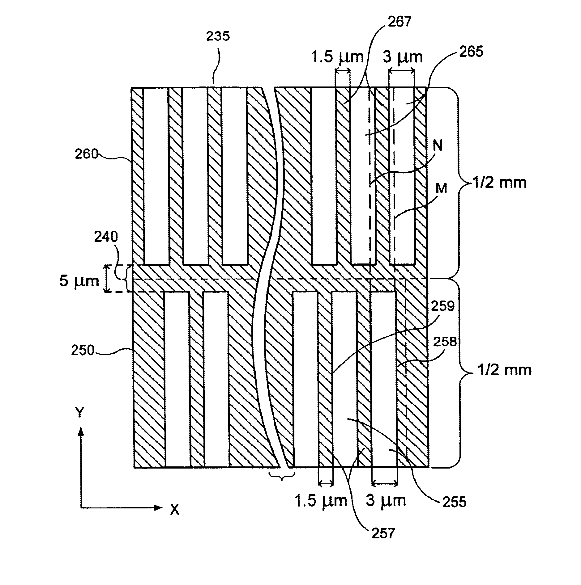
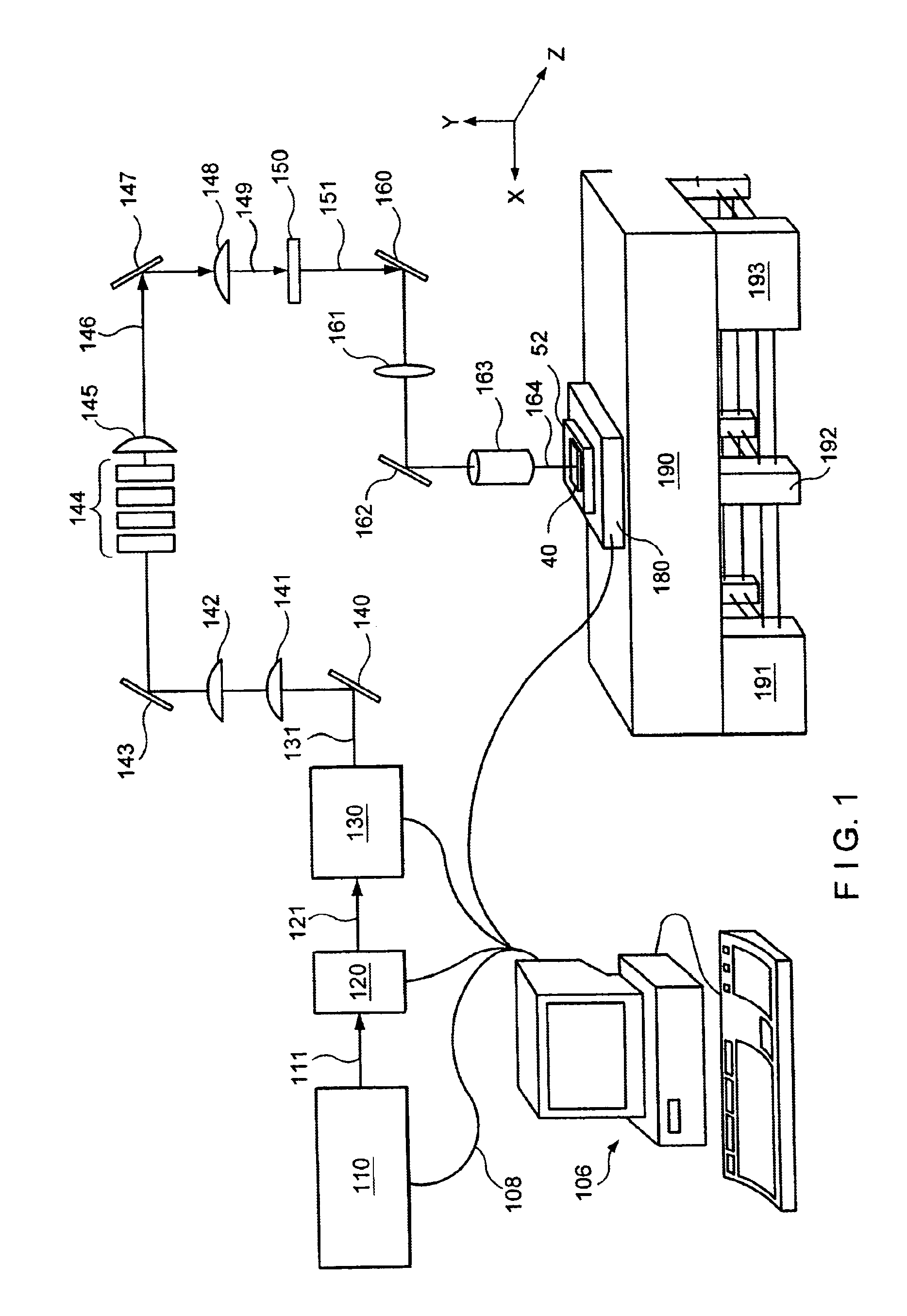
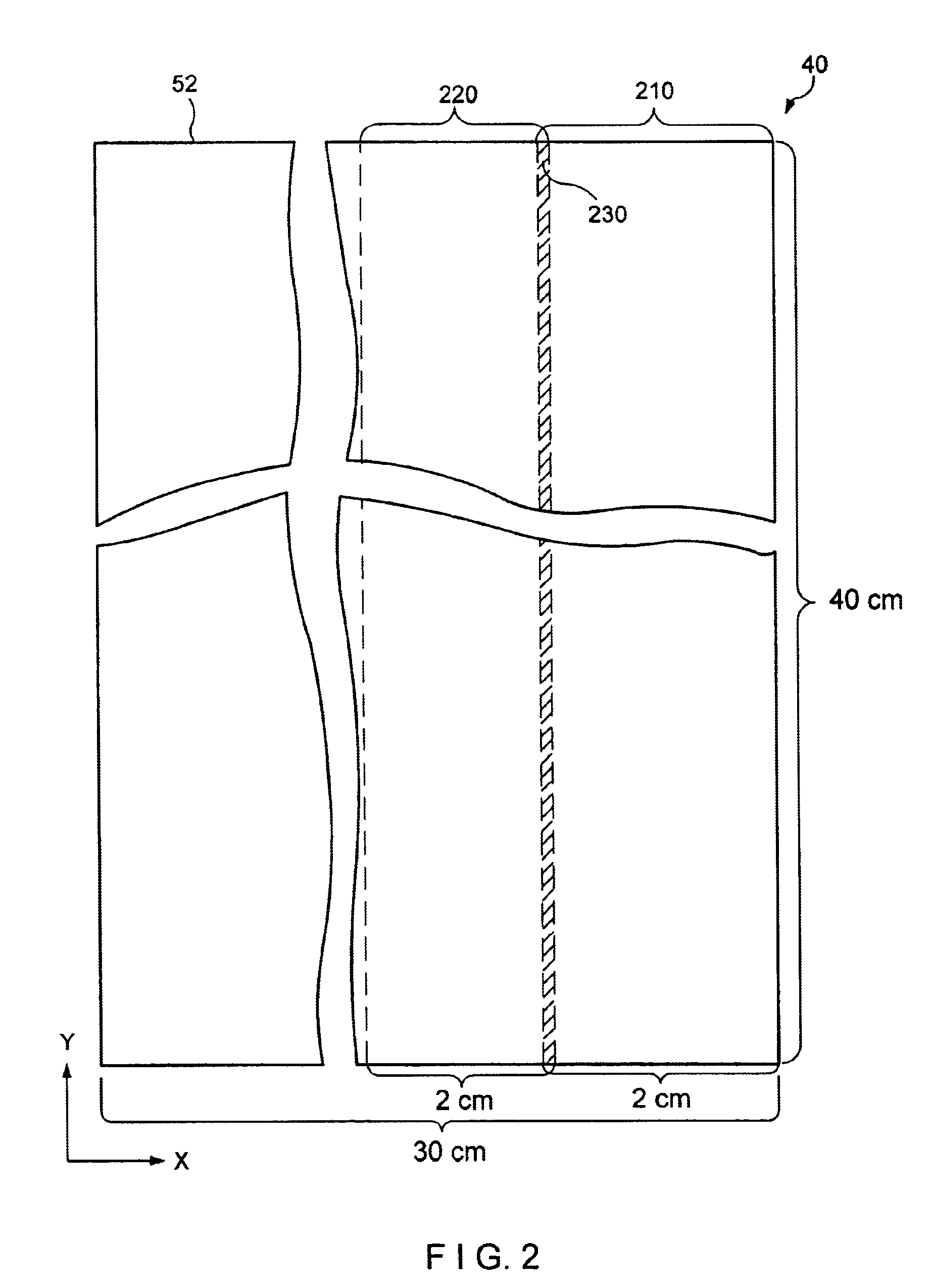
[0030]Certain systems and methods for providing a continuous motion SLS are described in U.S. patent application Ser. No. 09 / 526,585 (the “'585 application”), the entire disclosure of which is incorporated herein by reference. The '585 application explicitly describes and illustrates the details of these systems and methods, and their utilization of microtranslations of a sample, which has an amorphous silicon thin film provided thereon being irradiated by irradiation beam pulses to promote the sequential lateral solidification on the thin film. Similar to the system described in the '585 application, an exemplary embodiment of a system for carrying out the continuous motion SLS processing of amorphous silicon thin films according to the present invention is illustrated in FIG. 1. The exemplary system includes a Lambda Physik model LPX-315I XeCl pulsed excimer laser 110 emitting an irradiation beam (e.g., a laser beam), a controllable beam energy density modulator 120 for modifying ...
PUM
| Property | Measurement | Unit |
|---|---|---|
| Thickness | aaaaa | aaaaa |
| Speed | aaaaa | aaaaa |
| Width | aaaaa | aaaaa |
Abstract
Description
Claims
Application Information