Low voltage silicon controlled rectifier (SCR) for electrostatic discharge (ESD) protection of silicon-on-insulator technologies

a technology of electrostatic discharge and silicon-on-insulator, which is applied in the direction of semiconductor devices, semiconductor/solid-state device details, transistors, etc., can solve the problems of high cost of product repair, poor thermal conductivity of extremely thin active silicon film layer, and high esd problem. , to achieve the effect of low triggering and holding voltage, low impedance, and reducing voltage drop

Active Publication Date: 2005-06-21
SOFICS BVBA
View PDF11 Cites 116 Cited by
  • Summary
  • Abstract
  • Description
  • Claims
  • Application Information

AI Technical Summary

Benefits of technology

[0007]The disadvantages heretofore associated with the prior art are overcome by the present invention of a silicon-on-insulator (SOI) electrostatic discharge (ESD) protection device that can protect very sensitive thin gate oxides by limiting the power dissipation during the ESD event, which is best achieved by reducing the voltage drop across the active (protection) device during an ESD event. In one embodiment the invention provides very low triggering and holding voltages. Furthermore, the silicon-on-insulator (SOI) protection device of the present invention has low impedance and low power dissipation characteristics that reduce voltage build-up, and accordingly, enable designers to fabricate more area efficient protection devices.

Problems solved by technology

During installation of integrated circuits into products, these electrostatic discharges may destroy the IC's and thus require expensive repairs on the products, which could have been avoided by providing a mechanism for dissipation of the electrostatic discharge to which the IC may have been subjected.
The ESD problem has been especially pronounced in silicon-on-insulator (SOI) complementary metal oxide semiconductor (CMOS) field effect technologies, which require new considerations and approaches for ESD protection.
However, the thermal properties of the extremely thin active silicon film layer are poor in terms of thermal conductivity.
Specifically, silicon dioxide (SiO2) has a very poor thermal conductivity compared to silicon.
Therefore, when an ESD event occurs, heat generated at the ESD device (e.g., an SCR) can not be dissipated by the substrate.
Accordingly, during an ESD event, an active area of the ESD device is subject to excessive heat, which may cause damage to the ESD device.

Method used


Image

  • Low voltage silicon controlled rectifier (SCR) for electrostatic discharge (ESD) protection of silicon-on-insulator technologies
  • Low voltage silicon controlled rectifier (SCR) for electrostatic discharge (ESD) protection of silicon-on-insulator technologies
  • Low voltage silicon controlled rectifier (SCR) for electrostatic discharge (ESD) protection of silicon-on-insulator technologies

Examples


Embodiment Construction

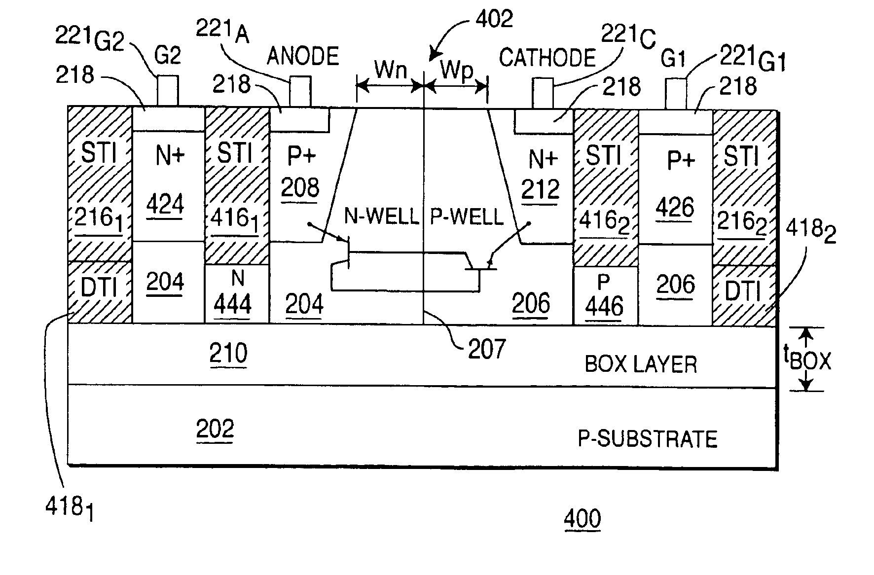
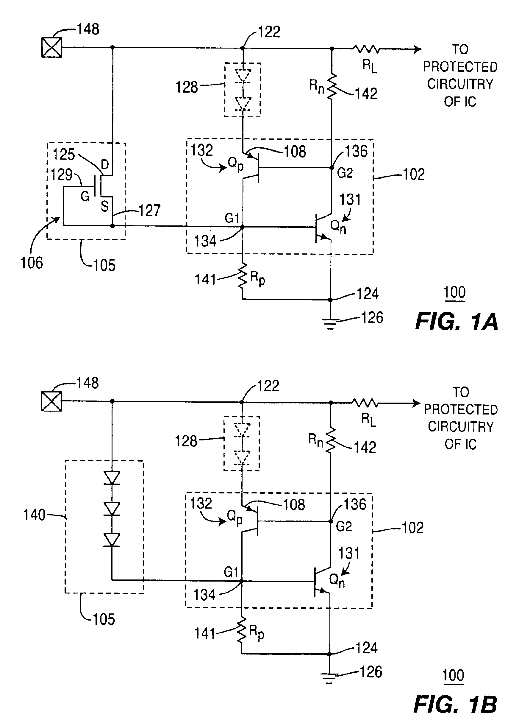
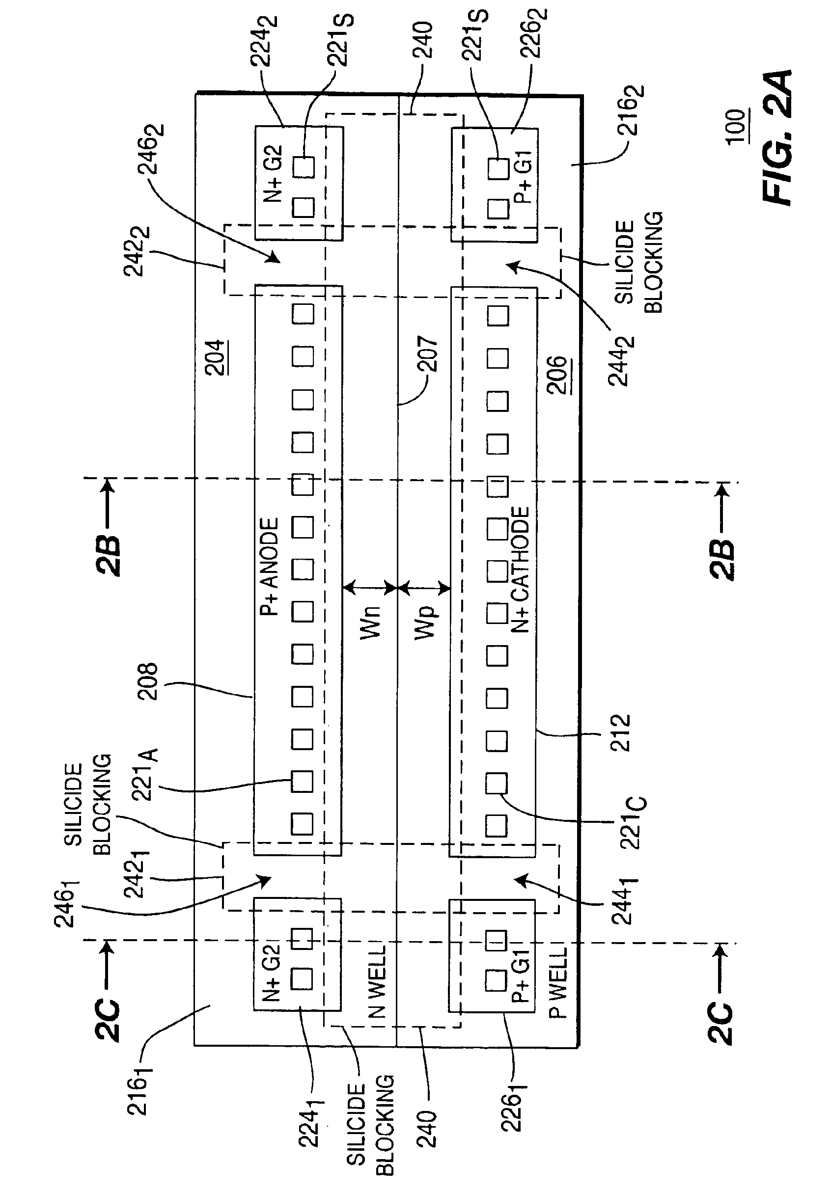
[0022]The process steps and structures described below do not form a complete process flow for manufacturing integrated circuits (ICs). The present invention can be practiced in conjunction with silicon-on-insulator (SOI) integrated circuit fabrication techniques currently used in the art, and only so much of the commonly practiced process steps are included as are necessary for an understanding of the present invention. The figures representing cross-sections and layouts of portions of an IC during fabrication are not drawn to scale, but instead are drawn so as to illustrate the important features of the invention. Furthermore, where possible, the figures illustratively include a schematic diagram of the circuitry (e.g., an SCR circuit) as related to the P and N-type doped regions of the integrated circuit.

[0023]The present invention is described with reference to SOI CMOS devices. However, those of ordinary skill in the art will appreciate that selecting different dopant types and...


PUM


Abstract

A silicon-on-insulator (SOI) electrostatic discharge (ESD) protection device that can protect very sensitive thin gate oxides by limiting the power dissipation during the ESD event, which is best achieved by reducing the voltage drop across the active (protection) device during an ESD event. In one embodiment, the invention provides very low triggering and holding voltages. Furthermore, the SOI protection device of the present invention has low impedance and low power dissipation characteristics that reduce voltage build-up, and accordingly, enable designers to fabricate more area efficient protection device

Description

CROSS REFERENCES[0001]This patent application claims the benefit of U.S. Provisional Application Ser. No. 60 / 463,461, filed Apr. 16, 2003, the contents of which are incorporated herein by reference in its entirety.FIELD OF THE INVENTION[0002]This invention generally relates to the field of electrostatic discharge (ESD) protection circuitry, and more specifically, for ESD protection for silicon-on-insulator (SOI) technologies.BACKGROUND OF THE INVENTION[0003]Integrated circuits (IC's) and other semiconductor devices are extremely sensitive to the high voltages that may be generated by contact with an ESD event. As such, electrostatic discharge (ESD) protection circuitry is essential for integrated circuits. An ESD event commonly results from the discharge of a high voltage potential (typically, several kilovolts) and leads to pulses of high current (several amperes) of a short duration (typically, 100 nanoseconds). An ESD event is generated within an IC, illustratively, by human cont...

Claims


Application Information

Patent Timeline
Patent Type & Authority Patents(United States)
IPC IPC(8): H01L29/74H01L29/66H01L27/02
CPCH01L29/7436H01L27/0262H01L23/60H01L23/62
Inventor RUSS, CORNELIUS CHRISTIANJOZWIAK, PHILLIP CZESLAWMERGENS, MARKUS PAUL JOSEFARMER, JOHNTRINH, CONG-SONMOHN, RUSSELLVERHAEGE, KOEN GERARD MARIA
Owner SOFICS BVBA
Why Eureka
Try Eureka