Nonplanar device with stress incorporation layer and method of fabrication

a technology of stress incorporation layer and non-planar transistor, which is applied in the direction of semiconductor devices, electrical devices, nanotechnology, etc., can solve the problems of increasing impracticality, decreasing the thickness of silicon film, and reducing the production efficiency of thin silicon film with less than 10 nanometer thicknesses, and is considered to be extremely difficul

Inactive Publication Date: 2005-06-21
INTEL CORP
View PDF13 Cites 241 Cited by
  • Summary
  • Abstract
  • Description
  • Claims
  • Application Information

AI Technical Summary

Benefits of technology

[0015]The present invention is novel non-planar or tri-gate transistor structure and its method of fabrication. The tri-gate transistor includes a stress film formed around the channel region of the device to provides a stress to the channel region to improve carrier mobility. Greater carrier mobility results in increased transistor drive current. In an embodiment of the present invention, the stress film is formed beneath the channel region so that it completely surrounds the channel. By completely surrounding the channel region with the stress film, the stress film provides stress to all sides of the channel, thereby providing stress over a large area and maximizing and improving device performance. The film stress properties, such a type of stress (i.e., compressive or tensile) and the amount of stress can be varied in order to optimize performance for different transistor types (e.g., PMOS and NMOS).
[0017]Because there are three separate channels formed in the semiconductor body, the semiconductor body can be fully depleted when the transistor is turned “ON”, thereby enabling the formation of a fully depleted transistor with gate lengths of less than 30 nanometers without requiring the use of ultra-thin semiconductor bodies or requiring photolithographic patterning of the semiconductor bodies to dimensions less than the gate length (Lg) of the device. That is, the structure of the tri-gate transistor of the present invention enables a fully depleted transistor to be fabricated where the thickness of the semiconductor body and width of the semiconductor body are equal to the gate length of the device. Because the novel tri-gate transistor of the present invention can be operated in a fully depleted manner, the device is characterized by ideal (i.e., very sharp) subthreshold slope and a reduced drain induced barrier lowering (DIBL) short channel effect of less than 100 mV / V and ideally about 60 mV / V which results in a lower leakage current when the device is turned “OFF” resulting in lower power consumption.

Problems solved by technology

However, as gate lengths scale especially as they approach 30 nm, the need for ever decreasing silicon film thickness (Tsi) makes this approach increasingly impractical.
The fabrication of thin silicon films with thicknesses of less than 10 nanometers, is considered to be extremely difficult.
On one hand, obtaining wafer uniformity on the order of one nanometer is a difficult challenge.
On the other hand, to be able to contact these thin films to form raised source / drain regions to decrease junction resistance, becomes almost impossible since the thin silicon layer in the source / drain regions becomes consumed during the gate etch and various cleans following the gate etch and spacer etch leaving insufficient silicon 106 for silicon to grow on.
Although, double gate structures double the thickness of the silicon film (since there now is a gate on either side of the channel) these structures, however, are hideously difficult to fabricate.

Method used


Image

  • Nonplanar device with stress incorporation layer and method of fabrication
  • Nonplanar device with stress incorporation layer and method of fabrication
  • Nonplanar device with stress incorporation layer and method of fabrication

Examples


Embodiment Construction

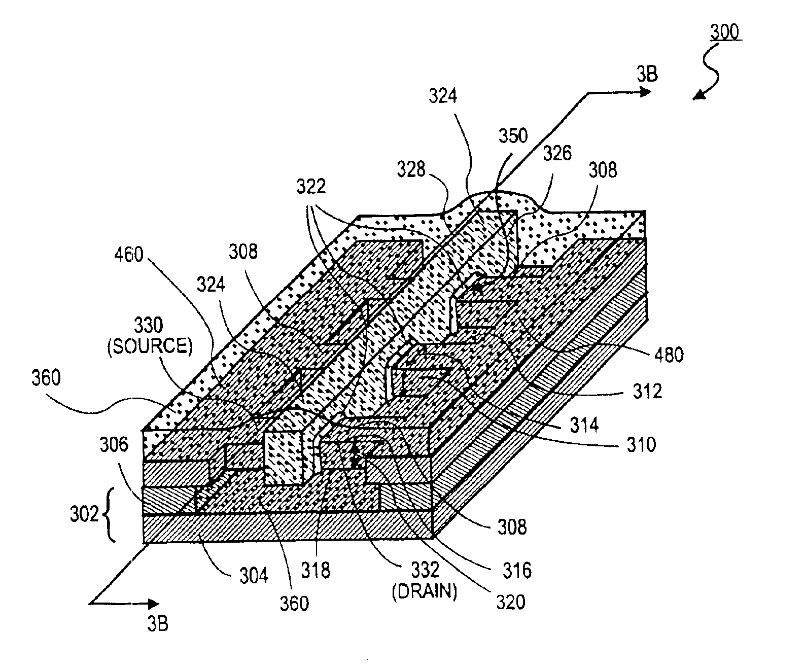
[0014]The present invention is a novel tri-gate or non-planar transistor structure with a stress incorporating layer and its method of fabrication. In the following description numerous specific details are set forth in order to provide a thorough understanding in the present invention. In other instances, well-known semiconductor process and manufacturing techniques have not been described in particular detail in order to not unnecessarily obscure the present invention.

[0015]The present invention is novel non-planar or tri-gate transistor structure and its method of fabrication. The tri-gate transistor includes a stress film formed around the channel region of the device to provides a stress to the channel region to improve carrier mobility. Greater carrier mobility results in increased transistor drive current. In an embodiment of the present invention, the stress film is formed beneath the channel region so that it completely surrounds the channel. By completely surrounding the c...


PUM


Abstract

A semiconductor device comprising a semiconductor body having a top surface and laterally opposite sidewalls is formed on an insulating substrate. A gate dielectric layer is formed on the top surface of the semiconductor body and on the laterally opposite sidewalls of the semiconductor body. A gate electrode is formed on the gate dielectric on the top surface of the semiconductor body and is formed adjacent to the gate dielectric on the laterally opposite sidewalls of the semiconductor body. A thin film is then formed adjacent to the semiconductor body wherein the thin film produces a stress in the semiconductor body.

Description

BACKGROUND OF THE INVENTION[0001]1. Field of the Invention[0002]The present invention relates to the field of semiconductor integrated circuit manufacturing and more specifically to a non-planar transistor having stress incorporation layer.[0003]2. Discussion of Related Art[0004]In order to increase device performance, silicon on insulator (SOI) transistors have been proposed for the fabrication of modern integrated circuits. FIG. 1 illustrates a standard fully depleted silicon on insulator (SOI) transistor 100. SOI transistor 100 includes a single crystalline silicon substrate 102 having an insulating layer 104, such as a buried oxide formed thereon. A single crystalline silicon body 106 is formed on the insulating layer 104. A gate dielectric layer 108 is formed on the single crystalline silicon body 106 and a gate electrode 110 formed on the gate dielectric 108. Source 112 and drain 114 regions are formed in the silicon body 106 along laterally opposite sides of gate electrode 11...

Claims


Application Information

Patent Timeline
Patent Type & Authority Patents(United States)
IPC IPC(8): H01L21/336H01L29/786H01L21/02H01L29/02H01L29/10H01L29/423H01L29/40H01L29/66H01L29/76
CPCH01L29/1054H01L29/42384H01L29/66628H01L29/7849H01L29/7842H01L29/7843H01L29/785H01L29/66795B82Y40/00H01L21/18
Inventor HARELAND, SCOTT A.CHAU, ROBERT S.DOYLE, BRIAN S.DATTA, SUMANJIN, BEEN-YIH
Owner INTEL CORP
Why Eureka
Try Eureka