Package structure of a composite LED

Inactive Publication Date: 2005-06-21
SOLIDLITE CORP
View PDF7 Cites 43 Cited by
  • Summary
  • Abstract
  • Description
  • Claims
  • Application Information

AI Technical Summary

Benefits of technology

[0014]The second method is to use a multi-chip package structure to produce the LED with greater brightness. In the second method, the electrode that needs a wire bonding process faces downward to cover the positive and negative electrodes in the recess by using a Filp Chip technology, so that the electrode needs not to be treated by a wire bonding process, and the volume may be reduced. In such a manner, the quality, wavelength and Vf of the chips are not distinguished, so that the chips easily cause problems in the manufacturing procedure.
[0015]The difference between the package process of the package structure of a composite LED of the present invention and that of the conventional high power multi-chip package structure is described as follows. In the present invention, multiple SMD LEDs are initially packaged. Then, the multiple packaged SMD LEDs are packaged into a larger package body. Thus, the quality of production is better. In addition, the wavelength, Vf and brightness of the LED chips may be classified before package of the SMD LEDs, thereby enhancing the convenience and choice of the LED procedure.

Problems solved by technology

The most important disturbance of the first conventional method for manufacturing a white LED is the color shift phenomenon.
In addition, the a

Method used


Image

  • Package structure of a composite LED
  • Package structure of a composite LED
  • Package structure of a composite LED

Examples


first embodiment

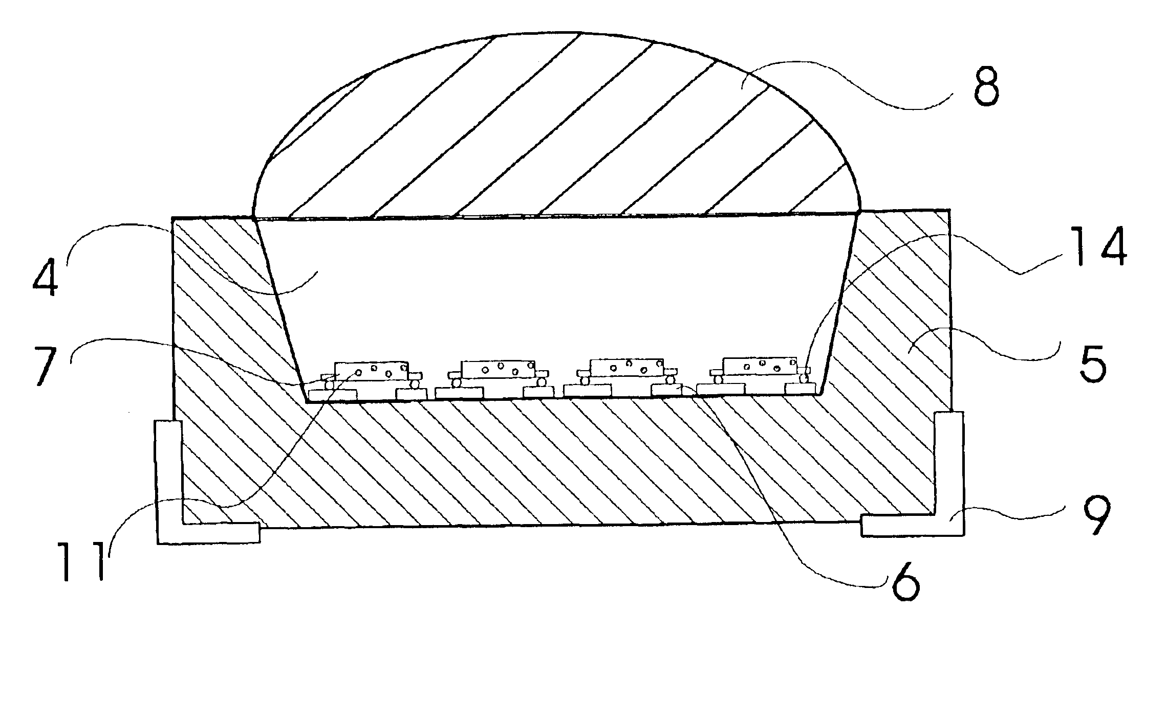
[0048]Referring to the drawings and initially to FIG. 4, a package structure of a composite LED in accordance with the present invention comprises an LED chip 1, a SMD package support 3, a phosphor 11, a package colloid (or epoxy) 4, a top light package support 5, two inner electrodes 6, and two top light outer electrodes 9.

[0049]The LED crystal 1 is a blue LED chip 1 (the wavelength is ranged between 430 nm and 470 nm) that may provide a light source and may excite the phosphor 11 to produce other wavelengths.

[0050]The phosphor 11 is a yellow phosphor 11 that may be used to absorb the blue light emitted from the blue LED chip 1, and may convert the blue light into the yellow light of a different wavelength. The yellow light and the blue light are complimentary with each other to produce the white light.

[0051]The manufacturing process of the package structure of a composite LED in accordance with the first embodiment of the present invention is described as follows.

[0052]First of al...

second embodiment

[0053]Referring to FIGS. 5 and 6, a package structure of a composite LED in accordance with the present invention comprises a SMD LED 7, a phosphor 11, a package colloid (or epoxy) 4, a side light package support 13, and a rectangular package 18 or an oblong package 19.

[0054]FIG. 5 is a schematic view of a rectangular package of the package structure of a composite LED in accordance with the second embodiment of the present invention, and FIG. 6 is a schematic view of an oblong package of the package structure of a composite LED in accordance with the second embodiment of the present invention.

[0055]The SMD LED 7 is a white light SMD LED 7 to provide a subbody of a white light source.

[0056]The side light package support 13 has an inside containing the rectangular package 18 or the oblong package 19, so that the side light package support 13 may function as a mother body of the package structure.

[0057]The manufacturing process of the package structure of a composite LED in accordance...

third embodiment

[0059]Referring to FIG. 7, a package structure of a composite LED in accordance with the present invention comprises a SMD LED 7, a phosphor 11, a package colloid (or epoxy) 4, a lamp type package support 10, a conducting wire 2, and a PCB 12.

[0060]The SMD LED 7 is a white SMD LED 7 to provide a subbody of a white light source.

[0061]The PCB 12 is a printed circuit board that may be used to support the SMD LED 7 and to connect the lamp type package support 10.

[0062]The manufacturing process of the package structure of a composite LED in accordance with the third embodiment of the present invention is the same as that of the package structure of a composite LED in accordance with the first embodiment of the present invention, and is described as follows.

[0063]The white SMD LED 7 is initially placed on the PCB 12, and is then placed in the package of the lamp type package support 10. The white SMD LED 7 is treated by a wire bonding process, so that the white SMD LED 7 is connected to t...


PUM


Abstract

A package structure of a composite LED is to package an LED chip into a SMD LED package subbody component. Then, a single SMD LED package subbody component or multiple SMD LED package subbody components may be packaged into a large sized recessed package mother body, thereby forming the package structure of a composite LED. Thus, the quality is better, and the color shift is less, thereby enhancing the quality of production, and thereby decreasing the cost of production. In addition, the SMD LED may be previously classified according to the features, and may then be packaged into the mother body, thereby obtaining better features, such as Vf, color, brightness or the like.

Description

BACKGROUND OF THE INVENTION[0001]1. Field of the Invention[0002]The present invention relates to a package structure of a composite LED, and more particularly to a package structure of a composite LED, wherein the quality is better, and the color shift is less, thereby enhancing the quality of production, and thereby decreasing the cost of production.[0003]2. Description of the Related Art[0004]In general, the LED (light emitting diode) has a long lifetime, can save the electric power, has a quick reaction velocity, has a high reliability, is environment protective, and may be used safely. The white LED is commonly used in the modern world.[0005]The conventional method for manufacturing a white LED adopts a single LED chip to produce the white light. The surface of the single LED chip is coated with a layer of phosphor, so that the light produced by the single LED chip may excite the phosphor, so as to produce rays with different wavelengths. The rays with different wavelengths may ...

Claims


Application Information

Patent Timeline
IPC IPC(8): H01L25/075H01L33/00H01L33/48
CPCH01L25/0753H01L33/486H01L2224/48091H01L2224/48247H01L2924/00014
Inventor CHEN, HSING
Owner SOLIDLITE CORP
Why Eureka
Try Eureka