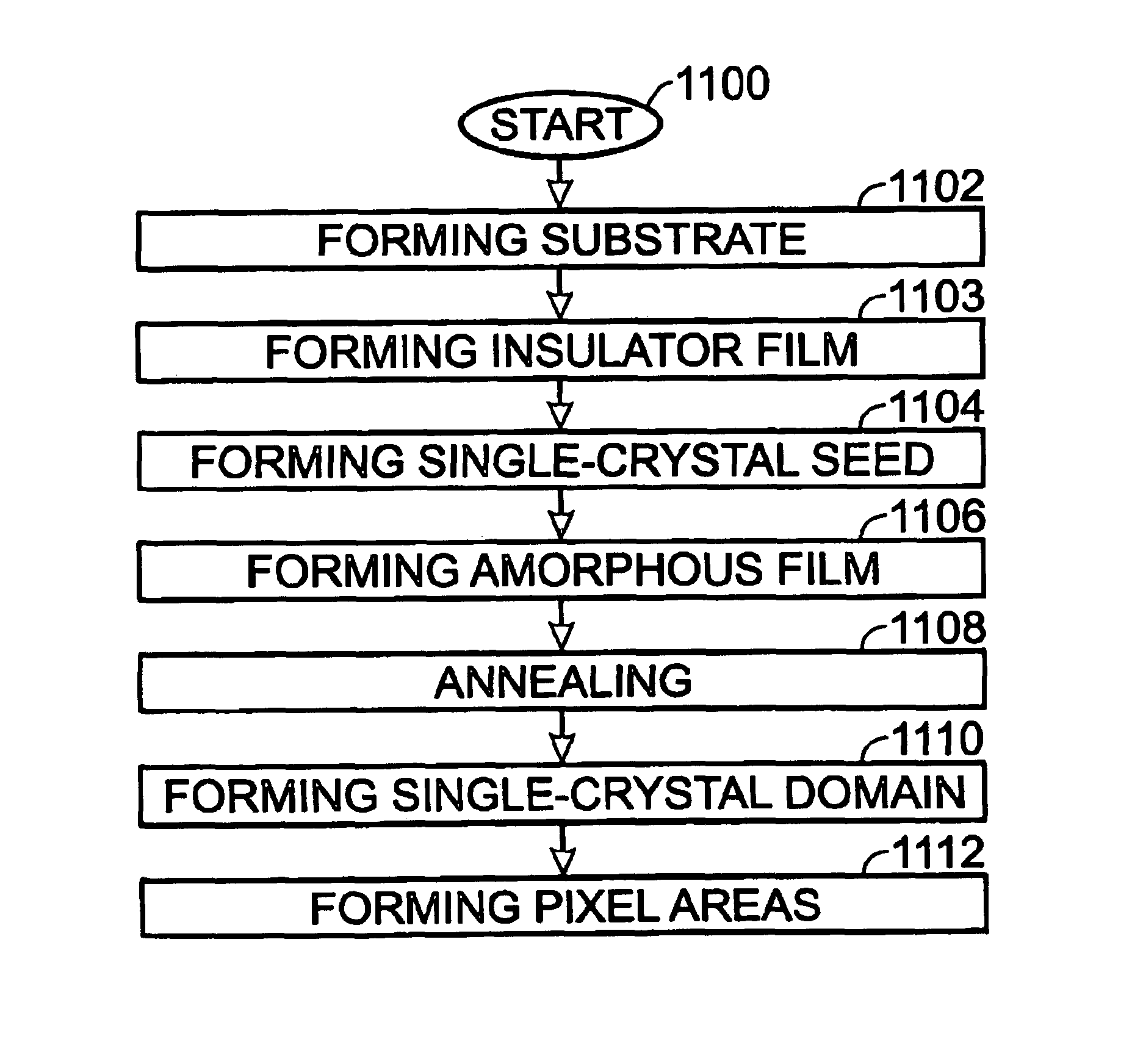
System and method for forming single-crystal domains using crystal seeds
a single crystal seed and crystal seed technology, applied in the direction of polycrystalline material growth, crystal growth process, chemically reactive gas, etc., can solve the problems of lack of uniformity between devices, insufficient to enable the fabrication of advanced circuits that offer low power consumption, high speed and other desirable characteristics, and non-uniform) content, etc., to achieve high-performance devices and uniform characteristics
- Summary
- Abstract
- Description
- Claims
- Application Information
AI Technical Summary
Benefits of technology
Problems solved by technology
Method used
Image

Examples
Embodiment Construction
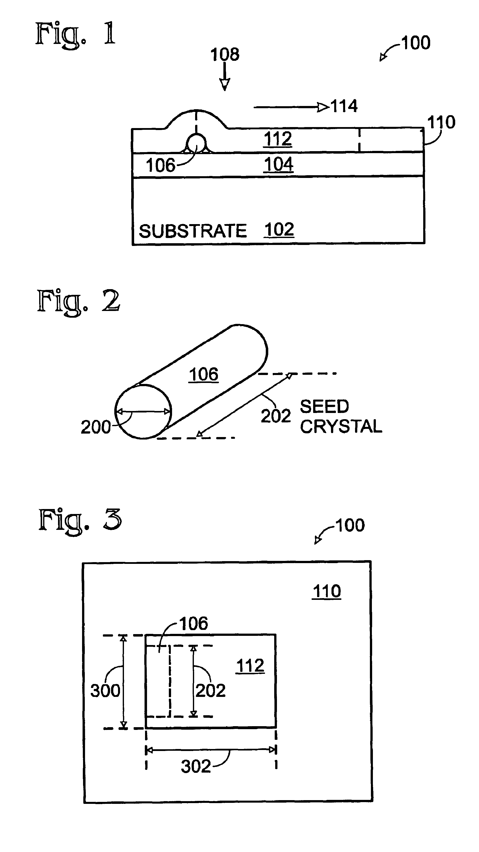
[0025]FIG. 1 is a partial cross-sectional view of the present invention semiconductor structure with lateral single-crystal domains. The structure 100 comprises a substrate 102. The substrate 102 can be a material such as glass, metal, plastic, or silicon. It can be advantageous to isolate the substrate 102 from the subsequently described semiconductor materials. In those instances, an insulator film 104 overlies the substrate 102 and underlies the single-crystal seed described below. The insulator film 104 can be formed from a material such as SiO2, SiNx, or combinations of SiO2 and SiNx, where x is in the range of 1 to 2.
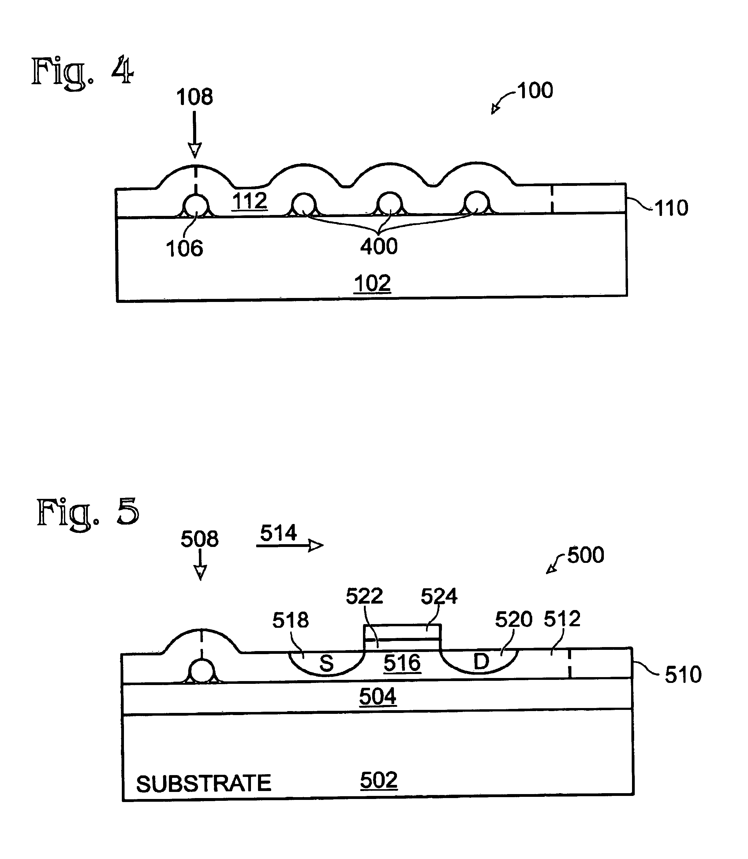
[0026]A first single-crystal seed 106 is shown having a location 108 overlying the substrate 102. A semiconductor film 110 overlies the substrate 102 and the first single-crystal seed 106. Typically, the semiconductor film 110 is a material such as Si or silicon germanium. However, other materials with structures capable of crystallization are also possible. The s...
PUM
| Property | Measurement | Unit |
|---|---|---|
| length | aaaaa | aaaaa |
| diameter | aaaaa | aaaaa |
| width | aaaaa | aaaaa |
Abstract
Description
Claims
Application Information