Method for forming shallow trench isolation structure
- Summary
- Abstract
- Description
- Claims
- Application Information
AI Technical Summary
Benefits of technology
Problems solved by technology
Method used
Image
Examples
Embodiment Construction
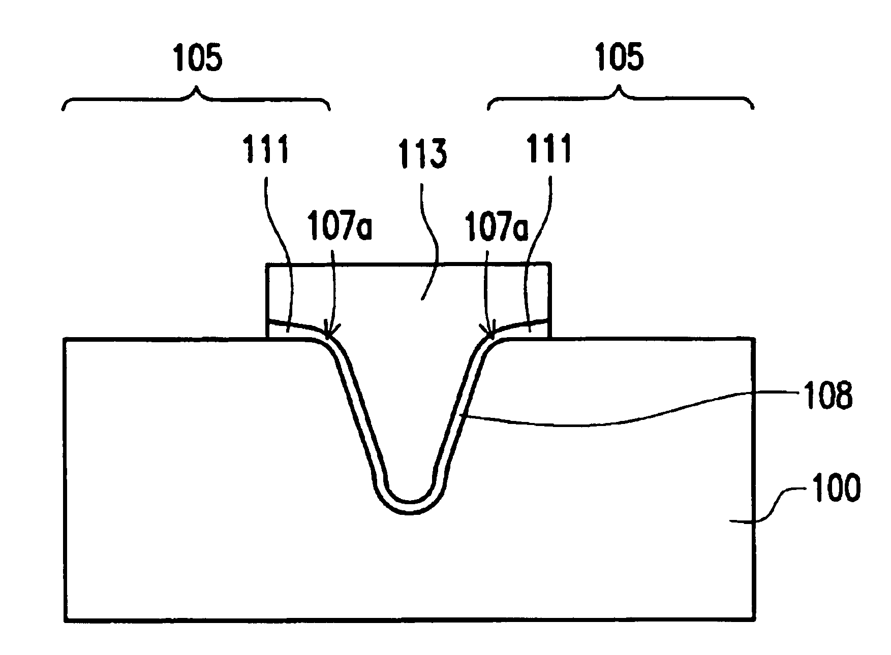
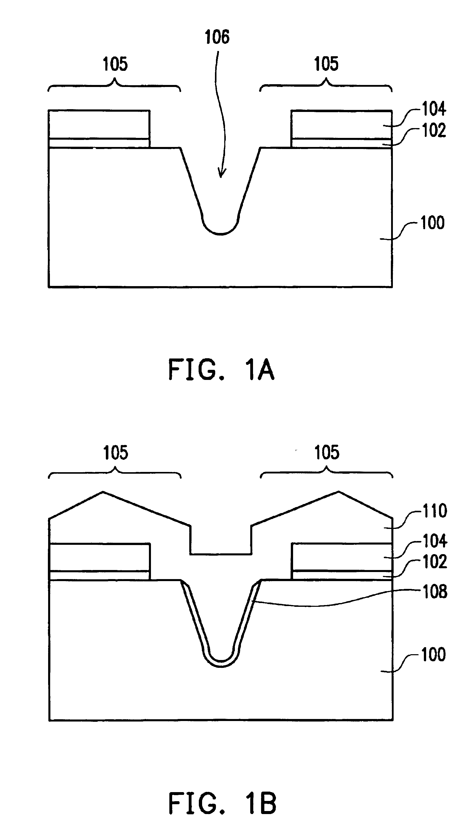
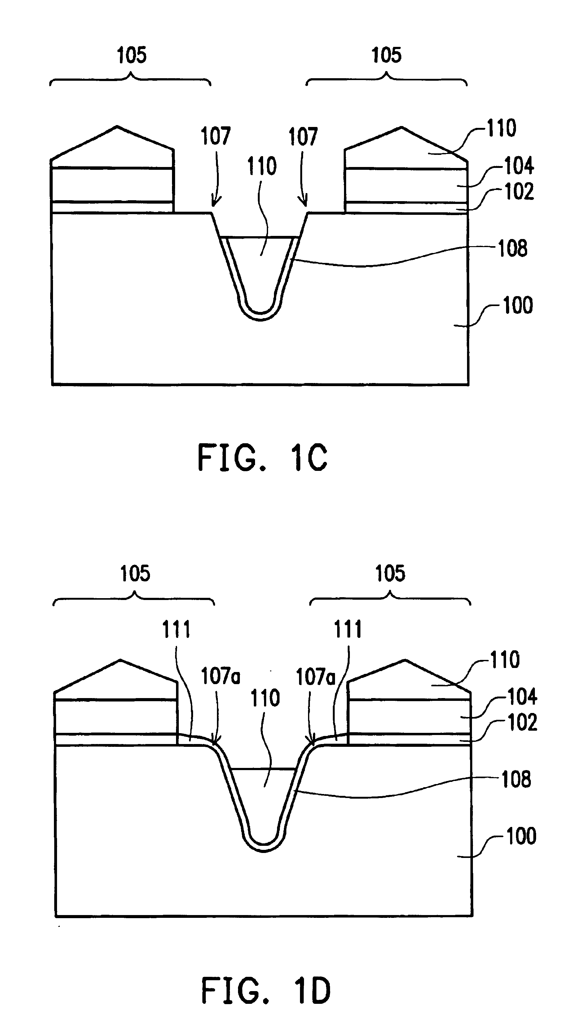
[0013]FIGS. 1A to 1F are cross-sectional views showing the process steps of fabricating a STI structure in accordance with a first preferred embodiment of the present invention. Referring to FIG. 1A, on a provided semiconductor substrate 100, for example, a silicon substrate, a pad oxide 102 layer is formed by thermal oxidation. A silicon nitride layer 104 is formed on the pad oxide layer 102 by, for example, rapid thermal chemical vapor deposition (RTCVD) with a thickness of 1000-2000 Angstroms. Next, forming a patterned first photoresist layer (not shown) is formed on the silicon nitride layer 104. Through conventional techniques of photolithography and etching, the silicon nitride layer 104 and the pad oxide layer 102 are patterned. Using the patterned first photoresist layer and the patterned silicon nitride layer 104 as a mask, the active regions 105 are defined and at least a shallow trench 106 is formed into the substrate 100. After removing the first photoresist layer, a sec...
PUM
 Abstract
Description
Claims
Application Information


