Method to form Cu/OSG dual damascene structure for high performance and reliable interconnects
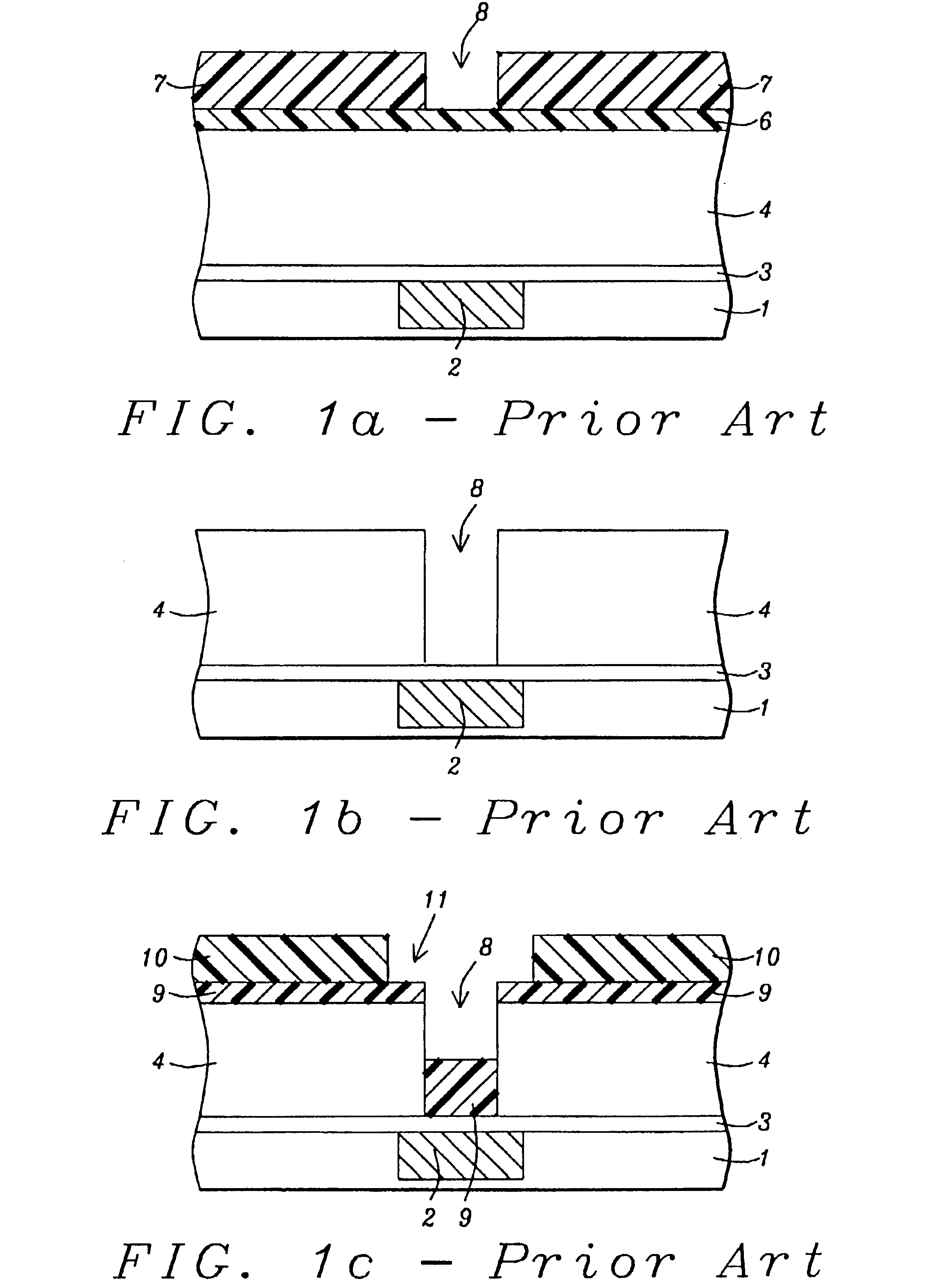
a damascene and dual-damascene technology, applied in the direction of semiconductor/solid-state device manufacturing, basic electric elements, electric apparatus, etc., can solve the problems of loss of reliability in the final device, material is susceptible to damage during the commonly used etching and cleaning steps, and the scheme is likely to be costly
- Summary
- Abstract
- Description
- Claims
- Application Information
AI Technical Summary
Benefits of technology
Problems solved by technology
Method used
Image
Examples
first embodiment
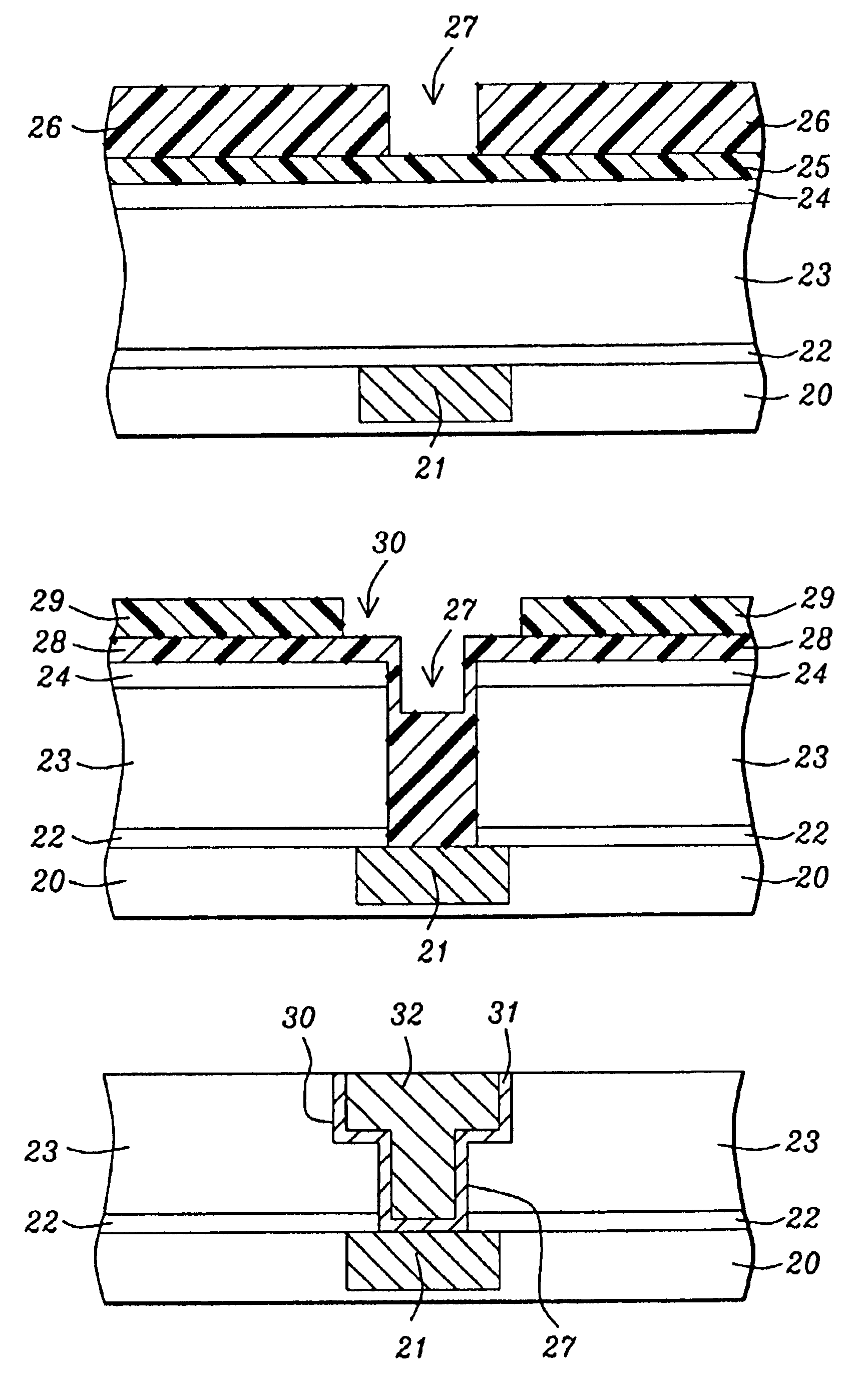
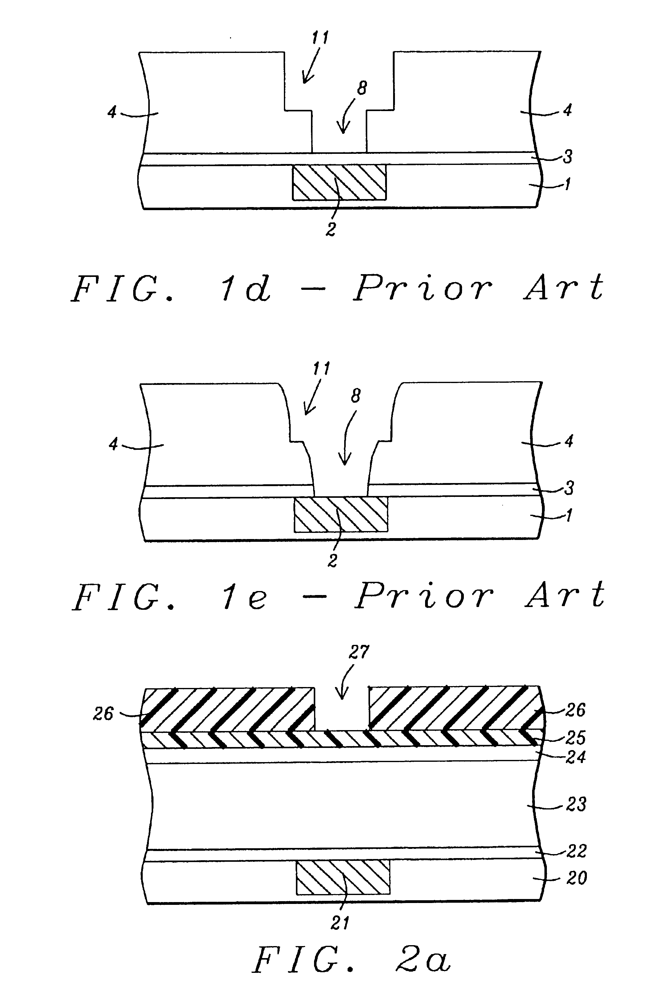
[0028]The present invention is particularly useful in forming a dual damascene structure that contains an OSG dielectric layer. The sequence of process steps is shown in a via first approach. A first embodiment is depicted in FIGS. 2a-2f. Although the figures depict a single OSG dielectric layer, it should be understood that the invention is also useful for a damascene stack that includes a capping layer on a substrate, a first OSG dielectric layer, an etch stop layer, and a second OSG dielectric layer on the etch stop.
[0029]Referring to FIG. 2a, a substrate 20 is provided that contains an exposed conductive layer 21 in an upper surface that will be used to construct a dual damascene structure. Substrate 20 is typically comprised of silicon or a silicon-germanium, gallium-arsenide, or silicon-on-insulator based technology. Substrate 20 is also comprised of active and passive devices that are not shown in order to simplify the drawings. Conductive layer 21 is preferably copper but ma...
second embodiment
[0043]An alternative via first approach for fabricating a dual damascene structure is illustrated in FIGS. 4a-4d as a Although the figures depict a single OSG dielectric layer, it should be understood that the invention is also useful for a damascene stack that includes a capping layer on a substrate, a first OSG dielectric layer, an etch stop layer, and a second OSG dielectric layer on the etch stop.
[0044]Referring to FIG. 4a, a substrate 40 is provided that contains an exposed conductive layer 41 in an upper surface that will be used to construct a dual damascene structure. Substrate 40 is typically comprised of silicon or a silicon-germanium, gallium-arsenide, or silicon-on-insulator based technology. Substrate 40 is also comprised of active and passive devices that are not shown in order to simplify the drawings. Conductive layer 41 is preferably copper but may also be a Cu / Al alloy, Al, or tungsten and is typically enclosed on the sides and bottom by a thin diffusion barrier l...
PUM
 Abstract
Description
Claims
Application Information


